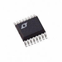
LTC3830EGN Linear Technology, LTC3830EGN Datasheet - Page 8

LTC3830EGN
Manufacturer Part Number
LTC3830EGN
Description
IC DC/DC CONTRLR STEP-DWN 16SSOP
Manufacturer
Linear Technology
Type
Step-Down (Buck)r
Datasheet
1.LTC3830ES8.pdf
(24 pages)
Specifications of LTC3830EGN
Internal Switch(s)
No
Synchronous Rectifier
Yes
Number Of Outputs
1
Voltage - Output
3.3V, Adj
Current - Output
20A
Frequency - Switching
200kHz
Voltage - Input
3 ~ 8 V
Operating Temperature
-40°C ~ 85°C
Mounting Type
Surface Mount
Package / Case
16-SSOP
Lead Free Status / RoHS Status
Contains lead / RoHS non-compliant
Power - Output
-
Available stocks
Company
Part Number
Manufacturer
Quantity
Price
Company:
Part Number:
LTC3830EGN
Manufacturer:
LT
Quantity:
10 000
Part Number:
LTC3830EGN
Manufacturer:
LINEAR
Quantity:
20 000
Company:
Part Number:
LTC3830EGN-8
Manufacturer:
LT
Quantity:
10 000
LTC3830/LTC3830-1
APPLICATIO S I FOR ATIO
TEST CIRCUITS
OVERVIEW
The LTC3830 is a voltage mode feedback, synchronous
switching regulator controller (see Block Diagram) de-
signed for use in high power, low voltage step-down
(buck) converters. It includes an onboard PWM generator,
a precision reference trimmed to ±0.8%, two high power
MOSFET gate drivers and all necessary feedback and
control circuitry to form a complete switching regulator
circuit. The PWM loop nominally runs at 200kHz.
The 16-lead versions of the LTC3830 include a current
limit sensing circuit that uses the topside external N-channel
power MOSFET as a current sensing element, eliminating
the need for an external sense resistor.
Also included in the 16-lead version and the LTC3830-1
is an internal soft-start feature that requires only a single
external capacitor to operate. In addition, 16-lead parts
feature an adjustable oscillator that can free run or
synchronize to external signal with frequencies from
100kHz to 500kHz, allowing added flexibility in external
component selection. The 8-lead version does not in-
clude current limit, internal soft-start and frequency
adjustability. The LTC3830-1 does not include current
limit, frequency adjustability, external synchronization
and the shutdown function.
8
NC
NC
NC
NC
FB
SS
FREQSET
COMP
I
MAX
V
SHDN
GND
SHDN
U
V
V
CC
CC
PGND
LTC3830
Figure 2
PV
U
CC2
SENSE
PV
PV
CC1
–
CC
SENSE
W
I
FB
3830 F02
+
G1
G2
6800pF
6800pF
U
THEORY OF OPERATION
Primary Feedback Loop
The LTC3830/LTC3830-1 sense the output voltage of the
circuit at the output capacitor and feeds this voltage back
to the internal transconductance error amplifier, ERR,
through a resistor divider network. The error amplifier
compares the resistor-divided output voltage to the inter-
nal 1.265V reference and outputs an error signal to the
PWM comparator. This error signal is compared with a
fixed frequency ramp waveform, from the internal oscil-
lator, to generate a pulse width modulated signal. This
PWM signal drives the external MOSFETs through the G1
and G2 pins. The resulting chopped waveform is filtered by
L
achieved with an external compensation network at the
COMP pin, the output node of the error amplifier.
MIN, MAX Feedback Loops
Two additional comparators in the feedback loop provide
high speed output voltage correction in situations where
the error amplifier may not respond quickly enough. MIN
compares the feedback signal to a voltage 40mV below the
internal reference. If the signal is below the comparator
threshold, the MIN comparator overrides the error ampli-
fier and forces the loop to maximum duty cycle, >91%.
O
V
and C
COMP
V
FB
OUT
COMP
FB
which closes the loop. Loop compensation is
I
MAX
I
FB
V
CC
LTC3830
GND
PV
Figure 3
5V
CC1
PGND
PV
CC2
G1
G2
+
3830 F03
10µF
6800pF
6800pF
G1 RISE/FALL
G2 RISE/FALL
0.1µF
3830fa


