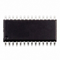
E-L6919ETR STMicroelectronics, E-L6919ETR Datasheet - Page 9

E-L6919ETR
Manufacturer Part Number
E-L6919ETR
Description
IC CTRLR 5BIT PROG 2PHASE 28SOIC
Manufacturer
STMicroelectronics
Type
Step-Down (Buck)r
Datasheet
1.E-L6919ETR.pdf
(33 pages)
Specifications of E-L6919ETR
Internal Switch(s)
No
Synchronous Rectifier
Yes
Number Of Outputs
1
Voltage - Output
0.8 ~ 1.55 V
Current - Output
2A
Frequency - Switching
150kHz
Voltage - Input
5 ~ 12 V
Operating Temperature
-40°C ~ 150°C
Mounting Type
Surface Mount
Package / Case
28-SOIC (7.5mm Width)
Power - Output
2W
Mounting Style
SMD/SMT
Operating Supply Voltage
6.5 V
Maximum Operating Temperature
85 C
Minimum Operating Temperature
- 40 C
Lead Free Status / RoHS Status
Lead free / RoHS Compliant
Other names
497-4592-2
Available stocks
Company
Part Number
Manufacturer
Quantity
Price
DIGITAL TO ANALOG CONVERTER
The built-in digital to analog converter allows the adjustment of the output voltage from 0.800V to 1.550V with
25mV as shown in the previous table 1. The internal reference is trimmed to ensure output voltage precision of
±0.6% and a zero temperature coefficient around 70°C. The internal reference voltage for the regulation is pro-
grammed by the voltage identification (VID) pins. These are TTL compatible inputs of an internal DAC that is
realized by means of a series of resistors providing a partition of the internal voltage reference. The VID code
drives a multiplexer that selects a voltage on a precise point of the divider. The DAC output is delivered to an
amplifier obtaining the V
provided (realized with a 5 A current generator up to 3.0V Typ); in this way, to program a logic "1" it is enough
to leave the pin floating, while to program a logic "0" it is enough to short the pin to GND. Programming the
"11111" code, the device enters the NOCPU mode: all mosfets are turned OFF and protections are disabled.
The condition is latched.
The voltage identification (VID) pin configuration also sets the power-good thresholds (PGOOD) and the Over
/ Under Voltage protection (OVP/UVP) thresholds.
DYNAMIC VID TRANSITION
The device is able to manage On-The-Fly VID Code changes that allow Output Voltage modification during nor-
mal device operation. The device checks every clock cycle (synchronously with the PWM ramp) for VID code
modifications. Once the new code is stable for more than one clock cycle, the reference steps up or down in
25mV increments every clock cycle until the new VID code is reached. During the transition, VID code changes
are ignored; the device re-starts monitoring VID after the transition has finished. PGOOD, signal is masked dur-
ing the transition and it is re-activated after the transition has finished while OVP / UVP are still active.
Figure 2. Dynamic VID transition
DRIVER SECTION
The integrated high-current drivers allow using different types of power MOS (also multiple MOS to reduce the
R
The drivers for the high-side mosfets use BOOTx pins for supply and PHASEx pins for return. The drivers for
the low-side mosfets use VCCDRV pin for supply and PGND pin for return. A minimum voltage of 4.6V at VC-
CDRV pin is required to start operations of the device.
The controller embodies a sophisticated anti-shoot-through system to minimize low side body diode conduction
time maintaining good efficiency saving the use of Schottky diodes. The dead time is reduced to few nanosec-
onds assuring that high-side and low-side mosfets are never switched on simultaneously: when the high-side
mosfet turns off, the voltage on its source begins to fall; when the voltage reaches 2V, the low-side mosfet gate
drive is applied with 30ns delay. When the low-side mosfet turns off, the voltage at LGATEx pin is sensed. When
it drops below 1V, the high-side mosfet gate drive is applied with a delay of 30ns. If the current flowing in the
inductor is negative, the source of high-side mosfet will never drop.
dsON
), maintaining fast switching transition.
PROG
Reference
voltage reference (i.e. the set-point of the error amplifier). Internal pull-ups are
V
VID
OUT
1 Clock Cycle Blanking Time
25mV steps transition
t
t
t
L6919E
9/33


