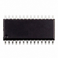
E-L6919ETR STMicroelectronics, E-L6919ETR Datasheet - Page 10

E-L6919ETR
Manufacturer Part Number
E-L6919ETR
Description
IC CTRLR 5BIT PROG 2PHASE 28SOIC
Manufacturer
STMicroelectronics
Type
Step-Down (Buck)r
Datasheet
1.E-L6919ETR.pdf
(33 pages)
Specifications of E-L6919ETR
Internal Switch(s)
No
Synchronous Rectifier
Yes
Number Of Outputs
1
Voltage - Output
0.8 ~ 1.55 V
Current - Output
2A
Frequency - Switching
150kHz
Voltage - Input
5 ~ 12 V
Operating Temperature
-40°C ~ 150°C
Mounting Type
Surface Mount
Package / Case
28-SOIC (7.5mm Width)
Power - Output
2W
Mounting Style
SMD/SMT
Operating Supply Voltage
6.5 V
Maximum Operating Temperature
85 C
Minimum Operating Temperature
- 40 C
Lead Free Status / RoHS Status
Lead free / RoHS Compliant
Other names
497-4592-2
Available stocks
Company
Part Number
Manufacturer
Quantity
Price
L6919E
Figure 3. Drivers peak current: High Side (left) and Low Side (right)
To allow the turning on of the low-side mosfet even in this case, a watchdog controller is enabled: if the source
of the high-side mosfet don't drop for more than 240ns, the low side mosfet is switched on so allowing the neg-
ative current of the inductor to recirculate. This mechanism allows the system to regulate even if the current is
negative.
The BOOTx and VCCDR pins are separated from IC's power supply (VCC pin) as well as signal ground (SGND
pin) and power ground (PGND pin) in order to maximize the switching noise immunity. The separated supply
for the different drivers gives high flexibility in mosfet choice, allowing the use of logic-level mosfet. Several com-
bination of supply can be chosen to optimize performance and efficiency of the application. Power conversion
is also flexible; 5V or 12V bus can be chosen freely.
The peak current is shown for both the upper and the lower driver of the two phases in figure 3. A 10nF capac-
itive load has been used. For the upper drivers, the source current is 1.9A while the sink current is 1.5A with
V
VCCDR = 12V.
CURRENT READING AND OVER CURRENT
The current flowing trough each phase is read using the voltage drop across the low side mosfets R
by the external resistor Rg placed outside the chip between ISENx and PGNDSx pins toward the reading points.
The full differential current reading rejects noise and allows to place sensing element in different locations with-
out affecting the measurement's accuracy. The current reading circuitry reads the current during the time in
which the low-side mosfet is on (OFF Time). During this time, the reaction keeps the pin ISENx and PGNDSx
at the same voltage while during the time in which the reading circuitry is off, an internal clamp keeps these two
pins at the same voltage sinking from the ISENx pin the necessary current (Needed if low-side mosfet R
sense is implemented to avoid absolute maximum rating overcome on ISENx pin).
The proprietary current reading circuit allows a very precise and high bandwidth reading for both positive and
negative current. This circuit reproduces the current flowing through the sensing element using a high speed
Track & Hold Tran conductance amplifier. In particular, it reads the current during the second half of the OFF
time reducing noise injection into the device due to the mosfet turn-on (See fig. 4). Track time must be at least
200ns to make proper reading of the delivered current
This circuit sources a constant 50 A current from the PGNDSx pin and keeps the pins ISENx and PGNDSx at
the same voltage. Referring to figure 4, the current that flows in the ISENx pin is then given by the following
equation:
10/33
across a sense resistor (R
BOOT -VPHASE
CH3 = HGATE1; CH4 = HGATE2
= 12V; similarly, for the lower drivers, the source current is 2.4A while the sink current is 2A with
SENSE
I
ISENx
) and internally converted into a current. The Tran conductance ratio is issued
=
50 A
+
R
----------------------------------------------
SENSE
R
g
I
PHASE
=
50 A
CH3 = LGATE1; CH4 = LGATE2
+
I
INFO x
dsON
dsON
or


