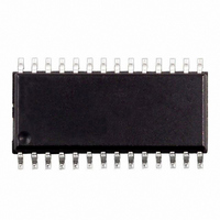
E-L6919ETR STMicroelectronics, E-L6919ETR Datasheet - Page 23

E-L6919ETR
Manufacturer Part Number
E-L6919ETR
Description
IC CTRLR 5BIT PROG 2PHASE 28SOIC
Manufacturer
STMicroelectronics
Type
Step-Down (Buck)r
Datasheet
1.E-L6919ETR.pdf
(33 pages)
Specifications of E-L6919ETR
Internal Switch(s)
No
Synchronous Rectifier
Yes
Number Of Outputs
1
Voltage - Output
0.8 ~ 1.55 V
Current - Output
2A
Frequency - Switching
150kHz
Voltage - Input
5 ~ 12 V
Operating Temperature
-40°C ~ 150°C
Mounting Type
Surface Mount
Package / Case
28-SOIC (7.5mm Width)
Power - Output
2W
Mounting Style
SMD/SMT
Operating Supply Voltage
6.5 V
Maximum Operating Temperature
85 C
Minimum Operating Temperature
- 40 C
Lead Free Status / RoHS Status
Lead free / RoHS Compliant
Other names
497-4592-2
Available stocks
Company
Part Number
Manufacturer
Quantity
Price
– An additional 100nF ceramic capacitor is suggested to place near HS mosfet drain. This helps in reduc-
– PHASE pin spikes. Since the HS mosfet switches in hard mode, heavy voltage spikes can be observed
Remote Buffer: The input connections for this components must be routed as parallel nets from the FBG/FBR
pins to the load in order to compensate losses along the output power traces and also to avoid the pick-up of
any common mode noise. Connecting these pins in points far from the load, will cause a non-optimum load reg-
ulation, increasing output tolerance.
Current Reading: The Rg resistor has to be placed as close as possible to the ISENx and PGNDSx pins in
order to limit the noise injection into the device. The PCB traces connecting these resistors to the reading point
must be routed as parallel traces in order to avoid the pick-up of any common mode noise. It's also important
to avoid any offset in the measurement and to get a better precision, to connect the traces as close as possible
to the sensing elements, dedicated current sense resistor or low side mosfet R
Moreover, when using the low side mosfet R
nected to the PHASEx pin. DO NOT CONNECT THE PINS TOGETHER AND THEN TO THE HS SOURCE!
The device won't work properly because of the noise generated by the return of the high side driver. In this case
route two separate nets: connect the PHASEx pin to the HS Source (route together with HGATEx) with a wide
net (30 mils) and the ISENx pin to the LS Drain (route together with PGNDSx). Moreover, the PGNDSx pin is
always connected, through the Rg resistor, to the PGND: DO NOT CONNECT DIRECTLY TO THE PGND! In
this case the device won't work properly. Route anyway to the LS mosfet source (together with ISENx net).
Right and wrong connections are reported in Figure 18.
Symmetrical layout is also suggested to avoid any unbalance between the two phases of the converter.
Figure 18. PCB layout connections for sense nets
ing noise.
on the PHASE pins. If these voltage spikes overcome the max breakdown voltage of the pin, the device
can absorb energy and it can cause damages. The voltage spikes must be limited by proper layout, the
use of gate resistors, Schottky diodes in parallel to the low side mosfets and/or snubber network on the
low side mosfets, to a value lower than 26V, for 20nSec, at FSW of 600kHz max.
Current Sense Connections.
Wrong (left) and correct (right) connections for the current reading sensing nets.
VIA to GND plane
NOT CORRECT
To PHASE
connection
dsON
as current sense element, the ISENx pin is practically con-
CORRECT
dsON
.
To LS Drain
and Source
To HS Gate
and Source
L6919E
23/33


