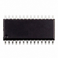
E-L6919ETR STMicroelectronics, E-L6919ETR Datasheet - Page 22

E-L6919ETR
Manufacturer Part Number
E-L6919ETR
Description
IC CTRLR 5BIT PROG 2PHASE 28SOIC
Manufacturer
STMicroelectronics
Type
Step-Down (Buck)r
Datasheet
1.E-L6919ETR.pdf
(33 pages)
Specifications of E-L6919ETR
Internal Switch(s)
No
Synchronous Rectifier
Yes
Number Of Outputs
1
Voltage - Output
0.8 ~ 1.55 V
Current - Output
2A
Frequency - Switching
150kHz
Voltage - Input
5 ~ 12 V
Operating Temperature
-40°C ~ 150°C
Mounting Type
Surface Mount
Package / Case
28-SOIC (7.5mm Width)
Power - Output
2W
Mounting Style
SMD/SMT
Operating Supply Voltage
6.5 V
Maximum Operating Temperature
85 C
Minimum Operating Temperature
- 40 C
Lead Free Status / RoHS Status
Lead free / RoHS Compliant
Other names
497-4592-2
Available stocks
Company
Part Number
Manufacturer
Quantity
Price
L6919E
or at least a portion of the total capacitance needed, has to be placed close to the power section in order to
eliminate the stray inductance generated by the copper traces. Low ESR and ESL capacitors are required.
Fig.16b shows some small signal components placement, and how and where to mix signal and power ground
planes. The distance from drivers and mosfet gates should be reduced as much as possible. Propagation delay
times as well as for the voltage spikes generated by the distributed inductance along the copper traces are so
minimized.
In fact, the further the mosfet is from the device, the longer is the interconnecting gate trace and as a conse-
quence, the higher are the voltage spikes corresponding to the gate PWM rising and falling signals. Even if
these spikes are clamped by inherent internal diodes, propagation delays, noise and potential causes of insta-
bilities are introduced jeopardizing good system behavior. One important consequence is that the switching
losses for the high side mosfet are significantly increased.
For this reason, it is suggested to have the device oriented with the driver side towards the mosfets and the
GATEx and PHASEx traces walking together toward the high side mosfet in order to minimize distance (see fig
17). In addition, since the PHASEx pin is the return path for the high side driver, this pin must be connected
directly to the High Side mosfet Source pin to have a proper driving for this mosfet.
For the LS mosfets, the return path is the PGND pin: it can be connected directly to the power ground plane (if
implemented) or in the same way to the LS mosfets Source pin. GATEx and PHASEx connections (and also
PGND when no power ground plane is implemented) must also be designed to handle current peaks in excess
of 2A (30 mils wide is suggested).
Gate resistors of few ohms help in reducing the power dissipated by the IC without compromising the system
efficiency.
Figure 17. Device orientation (left) and sense nets routing (right)
The placement of other components is also important:
– The bootstrap capacitor must be placed as close as possible to the BOOTx and PHASEx pins to mini-
– Decoupling capacitor from Vcc and SGND placed as close as possible to the involved pins.
– Decoupling capacitor from VCCDR and PGND placed as close as possible to those pins. This capacitor
– Refer to SGND all the sensible components such as frequency set-up resistor (when present) and also
– Connect SGND to PGND on the load side (output capacitor) to avoid undesirable load regulation effect
22/33
Power Connections Related.
mize the loop that is created.
sustains the peak currents requested by the low-side mosfet drivers.
the optional resistor from FB to GND used to give the positive droop effect.
and to ensure the right precision to the regulation when the remote sense buffer is not used.
Towards HS mosfet
Towards HS mosfet
Towards LS mosfet
(30 mils wide)
(30 mils wide)
(30 mils wide)
To regulated output
To LS mosfet
To LS mosfet
(or sense resistor)
(or sense resistor)


