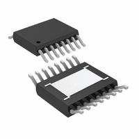
LT3695EMSE#PBF Linear Technology, LT3695EMSE#PBF Datasheet - Page 22

LT3695EMSE#PBF
Manufacturer Part Number
LT3695EMSE#PBF
Description
IC SWIT REG BUCK 1A ADJ 16MSOP
Manufacturer
Linear Technology
Type
Step-Down (Buck)r
Datasheet
1.LT3695EMSEPBF.pdf
(30 pages)
Specifications of LT3695EMSE#PBF
Internal Switch(s)
Yes
Synchronous Rectifier
No
Number Of Outputs
1
Voltage - Output
0.8 ~ 20 V
Current - Output
1A
Frequency - Switching
250kHz ~ 2.2MHz
Voltage - Input
3.6 ~ 36 V
Operating Temperature
-40°C ~ 125°C
Mounting Type
Surface Mount
Package / Case
16-MSOP Exposed Pad
Lead Free Status / RoHS Status
Lead free / RoHS Compliant
Power - Output
-
Available stocks
Company
Part Number
Manufacturer
Quantity
Price
APPLICATIONS INFORMATION
LT3695 Series
High Temperature Considerations
The PCB must provide heat sinking to keep the LT3695
regulators cool. The exposed pad on the bottom of the
package may be soldered to a copper area which should be
tied to large copper layers below with thermal vias; these
layers will spread the heat dissipated by the LT3695 regu-
lators. Place additional vias to reduce thermal resistance
further. With these steps, the thermal resistance from die
(or junction) to ambient can be reduced to θ
or less. With 100 LFPM airfl ow, this resistance can fall
by another 25%. Further increases in airfl ow will lead
to lower thermal resistance. Because of the large output
current capability of the LT3695 regulators, it is possible
to dissipate enough heat to raise the junction temperature
beyond the absolute maximum. When operating at high
ambient temperatures, the maximum load current should
be derated as the ambient temperature approaches these
maximums. If the junction temperature reaches the ther-
mal shutdown threshold, the parts will stop switching to
prevent internal damage due to overheating.
Power dissipation within the LT3695 regulators can be esti-
mated by calculating the total power loss from an effi ciency
measurement. The die temperature rise is calculated by
multiplying the power dissipation of the LT3695 regula-
tors by the thermal resistance from junction to ambient.
Die temperature rise was measured on a 2-layer, 10cm ×
10cm circuit board in still air at a load current of 1A (f
22
Figure 11. LT3695: The Dashed Lines Show Where a Connection
Would Occur if There Were an Inadvertent Short from RUN/SS
to an Adjacent Pin or from BOOST to BD. In These Cases, R3
Protects Circuitry Tied to the RT or SW Pins, and D2 Shields
BOOST from V
from SW
V
IN
R3
R
47Ω
SS
C
220nF
SS
OUT
R
T
. If C
RUN/SS
RT
V
IN
SS
LT3695
Is Used for Soft Start, R
BOOST
BD
SW
DA
FB
R2
C3 L1
D1
D2
R1
SS
JA
Isolates It
C2
= 40°C/W
3695 F11
R
LOAD
V
SW
OUT
=
800kHz). For a 12V input to 5V output the die temperature
elevation above ambient was 22°C with the exposed pad
soldered and 44°C without the exposed pad soldered.
Fault Tolerance
The LT3695 regulators are designed to tolerate single fault
conditions. Shorting two adjacent pins together or leaving
one single pin fl oating does not raise V
to the LT3695 regulators. However, the application circuit
must meet the requirements discussed in this section in
order to achieve this tolerance level.
Tables 5 and 6 show the effects that result from shorting
adjacent pins or from a fl oating pin, respectively.
For the best fault tolerance to inadvertent adjacent pin
shorts, the RUN/SS pin must not be directly connected to
either ground or V
and SW then connecting RUN/SS to V
to V
RUN/SS would tie SW to ground and would damage the
power switch if this is done when the power switch is on.
A short between RT and a RUN/SS pin that is connected
to V
RT pin. Therefore, the current supplying the RUN/SS pin
must be limited, for example, with resistor R3 in Figures
11 and 12. In case of a short between RUN/SS and SW this
resistor charges C2 through the inductor L1 if the current
it supplies from V
Figure 12. LT3695-3.3, LT3695-5: The Dashed Lines Show
Where a Connection Would Occur if There Were an Inadvertent
Short from RUN/SS to an Adjacent Pin. In These Cases, R3
Protects Circuitry Tied to the RT or SW Pins. R4 Provides an
Additional Load and May Be Necessary in Certain Situations
(See Text). If C
V
IN
IN
IN
would violate the absolute maximum ratings of the
and would thus raise V
R3
R
47Ω
SS
C
220nF
SS
SS
R
T
Is Used for Soft Start, R
RUN/SS
RT
IN
IN
V
LT3695-3.3
IN
LT3695-5
. If there was a short between RUN/SS
is not completely drawn by R
BOOST
OUT1
OUT2
SW
DA
OUT
. Likewise, grounding
C3 L1
D1
OUT
SS
R4
Isolates It from SW
IN
or cause damage
would tie SW
3695 F12
C2
LOAD
R
LOAD
V
OUT
3695fa
, R1


