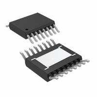
LT3695EMSE#PBF Linear Technology, LT3695EMSE#PBF Datasheet - Page 21

LT3695EMSE#PBF
Manufacturer Part Number
LT3695EMSE#PBF
Description
IC SWIT REG BUCK 1A ADJ 16MSOP
Manufacturer
Linear Technology
Type
Step-Down (Buck)r
Datasheet
1.LT3695EMSEPBF.pdf
(30 pages)
Specifications of LT3695EMSE#PBF
Internal Switch(s)
Yes
Synchronous Rectifier
No
Number Of Outputs
1
Voltage - Output
0.8 ~ 20 V
Current - Output
1A
Frequency - Switching
250kHz ~ 2.2MHz
Voltage - Input
3.6 ~ 36 V
Operating Temperature
-40°C ~ 125°C
Mounting Type
Surface Mount
Package / Case
16-MSOP Exposed Pad
Lead Free Status / RoHS Status
Lead free / RoHS Compliant
Power - Output
-
Available stocks
Company
Part Number
Manufacturer
Quantity
Price
APPLICATIONS INFORMATION
then the LT3695 regulators’ internal circuitry will pull its
quiescent current through its SW pin. This is fi ne if your
system can tolerate a few mA in this state. If you ground
the RUN/SS pin, the SW pin current will drop to essen-
tially zero. However, if the V
output is held high, then parasitic diodes inside the LT3695
regulators can pull large currents from the output through
the SW pin and the V
will run only when the input voltage is present and that
protects against a shorted or reversed input.
Figure 8. Diode D4 Prevents a Shorted Input from Discharging
a Backup Battery Tied to the Output. It Also Protects the Circuit
from a Reversed Input. The Regulator Runs Only When the Input
Is Present
V
IN
GND
Figure 9. A Good PCB Layout Ensures Proper,
Low EMI Operation (LT3695)
MBRS140
D4
R
V
T
IN
C2
V
RUN/SS
V
D1
IN
C
GND
IN
LT3695
PGND
BD
pin. Figure 8 shows a circuit that
C1
BOOST
V
FB
OUT
SW
IN
DA
L
pin is grounded while the
GND
R
C
C3
R2
R1
C
C
3695 F09
BACKUP
V
OUT
3695 F09
PCB Layout
For proper operation and minimum EMI, care must be
taken during printed circuit board layout. Figures 9 and
10 show the recommended component placement with
trace, ground plane and via locations. Note that large,
switched currents fl ow in the LT3695 regulators’ V
and PGND pins, the catch diode and the input capacitor
(C
as small as possible. These components, along with the
inductor and output capacitor (C
the same side of the circuit board, and their connections
should be made on that layer. All connections to GND should
be made at a common star ground point or directly to a
local, unbroken ground plane below these components.
The SW and BOOST nodes should be laid out carefully to
avoid interference. Finally, keep the FB, R
small so that the ground traces will shield them from the
SW and BOOST nodes. To keep thermal resistance low,
extend the ground plane as much as possible and add
thermal vias under and near the LT3695 regulators to any
additional ground planes within the circuit board and on the
bottom side. Keep in mind that the thermal design must
keep the junctions of the IC below the specifi ed absolute
maximum temperature.
IN
). The loop formed by these components should be
GND
Figure 10. A Good PCB Layout Ensures Proper,
Low EMI Operation (LT3695-3.3, LT3695-5)
R
V
IN
T
C2
D1
C1
V
OUT
L
LT3695 Series
OUT
GND
), should be placed on
C3
R
C
T
and V
C
C
C
21
IN
nodes
3695 F10
, SW
3695fa


