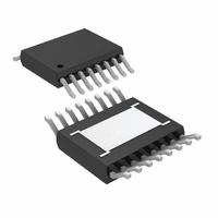
LT3695EMSE#PBF Linear Technology, LT3695EMSE#PBF Datasheet - Page 12

LT3695EMSE#PBF
Manufacturer Part Number
LT3695EMSE#PBF
Description
IC SWIT REG BUCK 1A ADJ 16MSOP
Manufacturer
Linear Technology
Type
Step-Down (Buck)r
Datasheet
1.LT3695EMSEPBF.pdf
(30 pages)
Specifications of LT3695EMSE#PBF
Internal Switch(s)
Yes
Synchronous Rectifier
No
Number Of Outputs
1
Voltage - Output
0.8 ~ 20 V
Current - Output
1A
Frequency - Switching
250kHz ~ 2.2MHz
Voltage - Input
3.6 ~ 36 V
Operating Temperature
-40°C ~ 125°C
Mounting Type
Surface Mount
Package / Case
16-MSOP Exposed Pad
Lead Free Status / RoHS Status
Lead free / RoHS Compliant
Power - Output
-
Available stocks
Company
Part Number
Manufacturer
Quantity
Price
APPLICATIONS INFORMATION
LT3695 Series
FB Resistor Network (LT3695)
The output voltage of the LT3695 is programmed with a
resistor divider between the output and the FB pin. Choose
the resistor values according to:
Reference designators refer to the Block Diagram of the
LT3695. 1% resistors are recommended to maintain output
voltage accuracy.
Setting the Switching Frequency
The LT3695 regulators use a constant-frequency PWM
architecture that can be programmed to switch from
250kHz to 2.2MHz by using a resistor tied from the RT
pin to ground. A table showing the necessary R
a desired switching frequency is in Table 1.
Table 1. Switching Frequency vs R
12
SWITCHING FREQUENCY (MHz)
R
1
=
R
2
⎛
⎜
⎝
0.25
V
0 8
0.3
0.4
0.5
0.6
0.7
0.8
0.9
1.0
1.2
1.4
1.6
1.8
2.0
2.2
OUT
.
V
−
1
⎞
⎟
⎠
T
Value
R
T
VALUE (kΩ)
90.9
71.5
57.6
47.5
40.2
29.4
22.6
18.2
14.7
12.1
9.76
8.06
158
127
34
T
value for
Operating Frequency Trade-Offs
Selection of the operating frequency is a trade-off between
effi ciency, component size, minimum dropout voltage and
maximum input voltage. The advantage of high frequency
operation is that smaller inductor and capacitor values may
be used. The disadvantages are lower effi ciency, lower
maximum input voltage and higher dropout voltage. The
highest acceptable switching frequency (f
given application can be calculated as follows:
where V
voltage, V
internal switch drop (~0.5V at max load). This equation
shows that lower switching frequency is necessary to
safely accommodate high V
in the Input Voltage Range section, lower frequency allows
a lower dropout voltage. Input voltage range depends on
the switching frequency because the LT3695 regulators’
switch has fi nite minimum on and off times. An internal
timer forces the switch to be off for at least t
cycle; this timer has a maximum value of 210ns (250ns
for T
turning off the power switch dictate the minimum on-time,
t
maximum value of 150ns over temperature. The minimum
and maximum duty cycles that can be achieved taking
minimum on and off times into account are:
where f
minimum switch on time (150ns), and t
minimum switch off time (210ns, 250ns for T
These equations show that the duty cycle range increases
when the switching frequency is decreased.
ON(MIN)
DC
DC
f
SW MAX
J
MIN
MAX
> 125°C). On the other hand, delays associated with
(
, before the switch can be turned off; t
SW
IN
D
= f
= 1 – f
is the typical input voltage, V
)
is the catch diode drop (~0.5V) and V
is the switching frequency, t
SW
=
t
t
ON MIN
ON(MIN)
SW
(
t
OFF(MIN)
V
)
(
OUT
V
IN
−
+
IN
V
/V
V
D
SW
OUT
+
ratio. Also, as shown
V
D
)
OUT
OFF(MIN)
SW(MAX)
ON(MIN)
is the output
ON(MIN)
OFF(MIN)
J
> 125°C).
SW
) for a
is the
is the
is the
has a
3695fa
per


