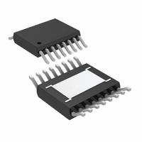
LT3695EMSE#PBF Linear Technology, LT3695EMSE#PBF Datasheet - Page 19

LT3695EMSE#PBF
Manufacturer Part Number
LT3695EMSE#PBF
Description
IC SWIT REG BUCK 1A ADJ 16MSOP
Manufacturer
Linear Technology
Type
Step-Down (Buck)r
Datasheet
1.LT3695EMSEPBF.pdf
(30 pages)
Specifications of LT3695EMSE#PBF
Internal Switch(s)
Yes
Synchronous Rectifier
No
Number Of Outputs
1
Voltage - Output
0.8 ~ 20 V
Current - Output
1A
Frequency - Switching
250kHz ~ 2.2MHz
Voltage - Input
3.6 ~ 36 V
Operating Temperature
-40°C ~ 125°C
Mounting Type
Surface Mount
Package / Case
16-MSOP Exposed Pad
Lead Free Status / RoHS Status
Lead free / RoHS Compliant
Power - Output
-
Available stocks
Company
Part Number
Manufacturer
Quantity
Price
APPLICATIONS INFORMATION
the circuit in Figure 4a. For higher output voltages, make
sure that there is no more than 8V at the BD pin either by
connecting it to another available supply higher than 3V or
by using a Zener diode between V
the BD pin voltage between 3V and 8V.
The minimum operating voltage of the LT3695 regulators
application is limited by the minimum input voltage and by
the maximum duty cycle as outlined previously. For proper
start-up, the minimum input voltage is also limited by the
boost circuit. If the input voltage is ramped slowly, or the
LT3695 regulators are turned on with their RUN/SS pin when
V
V
(4a) For V
V
IN
IN
IN
(4b) For 2.5V < V
Figure 4. Three Circuits for Generating
the Boost Voltage for the LT3695
(4c) For V
OUT
V
V
V
IN
IN
IN
GND
GND
GND
> 2.8V, V
LT3695
LT3695
LT3695
BD
BD
OUT
BD
PGND
PGND
BOOST
BOOST
PGND
BOOST
OUT
< 2.5V, V
SW
SW
SW
DA
DA
DA
IN(MIN)
< 2.8V, V
IN(MAX)
= 4.3V if V
C3
D1
C3
D1
OUT
C3
D1
IN(MIN)
D2
and BD to maintain
3695 F04a
3695 F04b
3695 F04c
= 25V
= 4.3V
OUT
V
V
V
< 3V
OUT
OUT
OUT
the output is already in regulation, then the boost capacitor
may not be fully charged. Because the boost capacitor is
charged with the energy stored in the inductor, the circuit
will rely on some minimum load current to get the boost
circuit running properly. This minimum load will depend
on input and output voltages, and on the arrangement of
the boost circuit. The minimum load generally goes to
zero once the circuit has started. Figure 5 shows a plot
of minimum load to start and to run as a function of input
voltage. In many cases the discharged output capacitor
will present a load to the switcher, which will allow it to
start. The plots show the worst-case situation where V
ramping very slowly. For lower start-up voltage, the boost
diode can be tied to V
range to one-half of the absolute maximum rating of the
BOOST pin. At light loads, the inductor current becomes
discontinuous and the effective duty cycle can be very high.
Figure 5. The Minimum Input Voltage Depends on
Output Voltage, Load Current and Boost Circuit
4.0
3.5
3.0
2.5
2.0
6.0
5.5
5.0
4.5
8.0
7.5
7.0
6.5
6.0
5.5
5.0
4.5
4.0
3.5
3.0
2.5
2.0
1
1
TO RUN
TO RUN
(WORST CASE)
(WORST CASE)
TO START
TO START
LOAD CURRENT (mA)
IN
LOAD CURRENT(mA)
10
10
; however, this restricts the input
LT3695 Series
100
100
V
T
L = 10μH
f = 800kHz
OUT
A
V
T
L = 10μH
f = 800kHz
A
= 25˚C
OUT
= 25˚C
= 3.3V
= 5V
3695 F05
1000
1000
19
3695fa
IN
is


