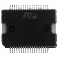
L6701TR STMicroelectronics, L6701TR Datasheet - Page 6

L6701TR
Manufacturer Part Number
L6701TR
Description
IC CTRLR 3PH VR10/9/K8 PWRSSO-36
Manufacturer
STMicroelectronics
Datasheet
1.L6701TR.pdf
(44 pages)
Specifications of L6701TR
Applications
Controller, Intel VR9, VR10, K8
Voltage - Input
12V
Number Of Outputs
3
Voltage - Output
0.8 ~ 1.85 V
Operating Temperature
0°C ~ 70°C
Mounting Type
Surface Mount
Package / Case
36-PowerSOIC
Output Voltage
0.8 V to 1.85 V
Output Current
1.5 A
Switching Frequency
110 KHz
Mounting Style
SMD/SMT
Maximum Operating Temperature
+ 125 C
Minimum Operating Temperature
0 C
Lead Free Status / RoHS Status
Lead free / RoHS Compliant
Other names
497-6108-2
2 Pins description and connection diagrams
Table 1.
6/44
Pin n
10
12
13
14
15
16
17
18
11
°
Pins description (continued)
OSC / EN /
DAC_SEL
SSEND /
UGATE2
PHASE2
UGATE3
PHASE3
PGOOD
BOOT2
BOOT3
FAULT
Name
Channel 2 HS driver supply.
Connect through a capacitor (100nF typ.) to PHASE2 and provide necessary
Bootstrap diode.
A small series resistor upstream the boot diode helps in reducing Boot capacitor
overcharge.
Channel 2 HS driver output.
A small series resistors helps in reducing device-dissipated power.
Channel 2 HS driver return path.
It must be connected to the HS2 MOSFET source and provides return path for
the HS driver of channel 2.
Channel 3 HS driver supply.
Connect through a capacitor (100nF typ.) to PHASE3 and provide necessary
Bootstrap diode.
A small series resistor upstream the boot diode helps in reducing Boot capacitor
overcharge.
Channel 3 HS driver output.
A small series resistors helps in reducing device-dissipated power.
Channel 3 HS driver return path.
It must be connected to the HS3 MOSFET source and provides return path for
the HS driver of channel 3.
SSEND - Intel VR10 Mode. Soft Start END Signal.
Open Drain Output set free after SS has finished and pulled low when triggering
any protection. Pull up to 5V (typ) or lower, if not used it can be left floating.
PGOOD - Intel VR9 & AMD Hammer Mode.
Open Drain Output set free after SS has finished and pulled low when VSEN is
lower than the relative threshold. Pull up to 5V (typ) or lower, if not used it can be
left floating.
DAC SELection pin.
It allows programming the DAC table for the regulation. Internally pulled-up to 5V.
Short to GND to program VR9 DAC, leave floating to program K8 DAC while
connect to GND through 82kΩ to program VR10 DAC.
Information about the selected DAC is latched before the system start-up. See
Section 7.1
OSC: It allows programming the switching frequency F
Switching frequency can be increased according to the resistor connected from
the pin vs. SGND with a gain of 4kHz/µA (see
floating it programs a switching frequency of 100kHz per phase (300kHz on the
load).
EN: Forced low, the device stops operations with all MOSFETs OFF: all the
protections are disabled except for
resets the device from any latching condition.
FAULT: The pin is forced high (5V) to signal an OVP / UVP FAULT: to recover
from this condition, cycle VCC or the OSC pin. See
for connections to enable CPU auto-detection.
Preliminary Over
Function
Section
Section 13
Voltage. When set low it
SW
14). Leaving the pin
of each channel.
for details.
L6701


