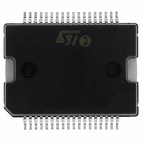
L6701TR STMicroelectronics, L6701TR Datasheet - Page 35

L6701TR
Manufacturer Part Number
L6701TR
Description
IC CTRLR 3PH VR10/9/K8 PWRSSO-36
Manufacturer
STMicroelectronics
Datasheet
1.L6701TR.pdf
(44 pages)
Specifications of L6701TR
Applications
Controller, Intel VR9, VR10, K8
Voltage - Input
12V
Number Of Outputs
3
Voltage - Output
0.8 ~ 1.85 V
Operating Temperature
0°C ~ 70°C
Mounting Type
Surface Mount
Package / Case
36-PowerSOIC
Output Voltage
0.8 V to 1.85 V
Output Current
1.5 A
Switching Frequency
110 KHz
Mounting Style
SMD/SMT
Maximum Operating Temperature
+ 125 C
Minimum Operating Temperature
0 C
Lead Free Status / RoHS Status
Lead free / RoHS Compliant
Other names
497-6108-2
L6701
15
System Control Loop Compensation
The control loop is composed by the Current Sharing control loop (See
Average Current Mode control loop. Each loop gives, with a proper gain, the correction to the
PWM in order to minimize the error in its regulation: the Current Sharing control loop equalize
the currents in the inductors while the Average Current Mode control loop fixes the output
voltage equal to the reference programmed by VID.
system control loop.
The system Control Loop is reported in
the DROOP pin flows into R
read current.
Figure 17. Main Control Loop
The system can be modeled with an equivalent single phase converter which only difference is
the equivalent inductor L/3 (where each phase has an L inductor).The Control Loop gain results
(obtained opening the loop after the COMP pin):
Where:
(
Z
the applied load R
Z
Z
A(s) is the error amplifier gain;
R
P
F
L
D ROOP
R
(s) is the compensation network impedance;
(s) is the parallel of the three inductor impedance;
(s) is the impedance resulting by the parallel of the output capacitor (and its ESR) and
DROO P
=
DCR
------------- R
R
=
G
D
CURRENT SHARING
3
LOO P
CORRECTION
DUTY CYCLE
⋅
⋅
DCR
------------ - R
1 / 5
1 / 5
1 / 5
O
R
FB
;
s ( )
D
is the equivalent output resistance determined by the droop function
FB
⋅
=
implementing the dependence of the output voltage from the
FB
–
------------------------------------------------------------------------------------------------------------------- -
[
Z
P
for fully differential current sense);
I
I
I
s ( )
INFO1
INFO2
INFO3
PWM Z
Figure
+
Z
PWM3
PWM2
PWM1
L
4 / 5
⋅
s ( )
ERROR AMPLIFIER
18. The current information I
F
]
s ( )
COMP
⋅
Z
-------------- -
⋅
A s ( )
Figure 17
F
(
R
s ( )
DROOP
L3
L2
L1
Z
+
F
(s)
15 System Control Loop Compensation
⎛
⎝
1
+
shows the block diagram of the
Reference
FB
+
----------- -
A s ( )
Z
1
P
s ( )
⎞ R
⎠
I
DROOP
⋅
C
)
Figure
OUT
FB
Z
F
DROOP
(s)
R
OUT
17) and the
sourced by
35/44


