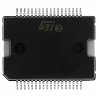
L6701TR STMicroelectronics, L6701TR Datasheet - Page 18

L6701TR
Manufacturer Part Number
L6701TR
Description
IC CTRLR 3PH VR10/9/K8 PWRSSO-36
Manufacturer
STMicroelectronics
Datasheet
1.L6701TR.pdf
(44 pages)
Specifications of L6701TR
Applications
Controller, Intel VR9, VR10, K8
Voltage - Input
12V
Number Of Outputs
3
Voltage - Output
0.8 ~ 1.85 V
Operating Temperature
0°C ~ 70°C
Mounting Type
Surface Mount
Package / Case
36-PowerSOIC
Output Voltage
0.8 V to 1.85 V
Output Current
1.5 A
Switching Frequency
110 KHz
Mounting Style
SMD/SMT
Maximum Operating Temperature
+ 125 C
Minimum Operating Temperature
0 C
Lead Free Status / RoHS Status
Lead free / RoHS Compliant
Other names
497-6108-2
8 Driver Section
8
8.1
18/44
Driver Section
The integrated high-current drivers allow using different types of power MOS (also multiple
MOS to reduce the equivalent R
The drivers for the high-side MOSFETs use BOOTx pins for supply and PHASEx pins for
return. The drivers for the low-side MOSFETs use the VCC pin for supply and PGND pin for
return.
The controller embodies a anti-shoot-through and adaptive dead-time control to minimize low
side body diode conduction time maintaining good efficiency saving the use of Schottky diodes:
when the high-side MOSFET turns off, the voltage on its source begins to fall; when the voltage
reaches 2V, the low-side MOSFET gate drive is suddenly applied. When the low-side MOSFET
turns off, the voltage at LGATEx pin is sensed. When it drops below 1V, the high-side MOSFET
gate drive is suddenly applied. If the current flowing in the inductor is negative, the source of
high-side MOSFET will never drop. To allow the low-side MOSFET to turn-on even in this case,
a watchdog controller is enabled: if the source of the high-side MOSFET does not drop, the low
side MOSFET is switched on so allowing the negative current of the inductor to recirculate. This
mechanism allows the system to regulate even if the current is negative.
Power conversion input is flexible: 5V, 12V bus or any bus that allows the conversion (See
maximum duty cycle limitations) can be chosen freely.
Power Dissipation
L6701 embeds high current MOSFET drivers for both high side and low side MOSFETs: it is
then important to consider the power that the device is going to dissipate in driving them in
order to avoid overcoming the maximum junction operative temperature. In addition, since the
device has an exposed pad to better dissipate the power, the thermal resistance between
junction and ambient consequent to the layout is also important: thermal pad need to be
soldered to the PCB ground plane through several VIAs in order to facilitate the heat
dissipation.
Two main terms contribute in the device power dissipation: bias power and drivers' power.
External gate resistors helps the device to dissipate the switching power since the same power
P
a general cooling of the device.
SW
Device Power (P
pins and it is simply quantifiable as follow (assuming to supply HS and LS drivers with the
same VCC of the device):
Drivers' power is the power needed by the driver to continuously switch on and off the
external MOSFETs; it is a function of the switching frequency and total gate charge of the
selected MOSFETs. It can be quantified considering that the total power P
switch the MOSFETs (easy calculable) is dissipated by three main factors: external gate
resistance (when present), intrinsic MOSFET resistance and intrinsic driver resistance.
This last term is the important one to be determined to calculate the device power
dissipation. The total power dissipated to switch the MOSFETs results:
will be shared between the internal driver impedance and the external resistor resulting in
P
DC
SW
) depends on the static consumption of the device through the supply
P
DC
=
3 F
=
⋅
DS(on)
V
SW
CC
⋅
⋅
), maintaining fast switching transition.
(
(
Q
I
CC
G HS
+
3 I
⋅
V
⋅
BO OT
CCDRx
+
+
Q
3 I
GLS
⋅
BOO Tx
⋅
V
CCDRx
)
)
SW
dissipated to
L6701


