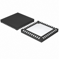
MAX1544ETL+ Maxim Integrated Products, MAX1544ETL+ Datasheet - Page 35

MAX1544ETL+
Manufacturer Part Number
MAX1544ETL+
Description
IC QUICK-PWM DUAL-PHASE 40-TQFN
Manufacturer
Maxim Integrated Products
Series
Quick-PWM™r
Datasheet
1.MAX1544ETLT.pdf
(42 pages)
Specifications of MAX1544ETL+
Applications
Controller, AMD Hammer
Voltage - Input
2 ~ 28 V
Number Of Outputs
1
Voltage - Output
0.68 ~ 1.55 V
Operating Temperature
-40°C ~ 100°C
Mounting Type
Surface Mount
Package / Case
40-TQFN Exposed Pad
Output Voltage
0.675 V to 1.55 V
Output Current
40 A
Input Voltage
4 V to 28 V
Mounting Style
SMD/SMT
Maximum Operating Temperature
+ 100 C
Minimum Operating Temperature
- 40 C
Lead Free Status / RoHS Status
Lead free / RoHS Compliant
medium-sized MOSFETs. However, high-current appli-
cations driving large, high-side, MOSFETs require
boost capacitors larger than 0.1µF. For these applica-
tions, select the boost capacitors to avoid discharging
the capacitor more than 200mV while charging the
high-side MOSFET’s gates:
where N is the number of high-side MOSFETs used for
one regulator, and Q
the MOSFET’s data sheet. For example, assume two
IRF7811W N-channel MOSFETs are used on the high
side. According to the manufacturer’s data sheet, a
single IRF7811W has a maximum gate charge of 24nC
(V
capacitance would be:
Selecting the closest standard value, this example
requires a 0.22µF ceramic capacitor.
The current-balance compensation capacitor (C
integrates the difference between the main and sec-
ondary current-sense voltages. The internal compensa-
tion resistor (R
by increasing the phase margin. This allows the
dynamics of the current balance loop to be optimized.
Excessively large capacitor values increase the inte-
gration time constant, resulting in larger current differ-
ences between the phases during transients.
Excessively small capacitor values allow the current
loop to respond cycle-by-cycle but can result in small
DC current variations between the phases. Likewise,
excessively large resistor values can also cause DC
current variations between the phases. Small resistor
values reduce the phase margin, resulting in marginal
stability in the current-balance loop. For most applica-
tions, a 470pF capacitor from CCI to the switching reg-
ulator’s output works well.
Connecting the compensation network to the output
(V
voltage signal, especially during transients. To reduce
noise pickup in applications that have a widely distrib-
uted layout, it is sometimes helpful to connect the com-
pensation network to the quiet analog ground rather
than V
GS
OUT
= 5V). Using the above equation, the required boost
) allows the controller to feed forward the output
OUT
Current-Balance Compensation (CCI)
.
CCI
C
BST
C
= 20kΩ) improves transient response
______________________________________________________________________________________
BST
AMD Hammer CPU Core Power Supplies
GATE
=
=
2
Dual-Phase, Quick-PWM Controller for
200
N x Q
x
is the gate charge specified in
200
24
mV
nC
mV
GATE
=
0 24
.
µ
F
CCI
)
Voltage positioning dynamically lowers the output volt-
age in response to the load current, reducing the
processor’s power dissipation. When the output is
loaded, an operational amplifier (Figure 5) increases
the signal fed back to the Quick-PWM controller’s feed-
back input. The adjustable amplification allows the use
of standard, current-sense resistor values, and signifi-
cantly reduces the power dissipated since smaller cur-
rent-sense resistors can be used. The load transient
response of this control loop is extremely fast, yet well
controlled, so the amount of voltage change can be
accurately confined within the limits stipulated in the
microprocessor power-supply guidelines.
The voltage-positioned circuit determines the load current
from the voltage across the current-sense resistors
(R
and output capacitors, as shown in Figure 10. The voltage
drop can be determined by the following equation:
where η
for voltage-positioning feedback, and η
number of active phases. When the slave controller is
disabled, the current-sense summation maintains the
proper voltage-positioned slope. Select the positive
input summing resistors so R
The nonadjustable minimum off-time one-shot and the
number of phases restrict the output voltage adjustable
range for continuous-conduction operation. For best
dropout performance, use the slower (200kHz) on-time
settings. When working with low input voltages, the
duty-factor limit must be calculated using worst-case
values for on- and off-times. Manufacturing tolerances
and internal propagation delays introduce an error to
the TON K factor. This error is greater at higher fre-
quencies (Table 6). Also, keep in mind that transient
response performance of buck regulators operated too
close to dropout is poor, and bulk output capacitance
must often be added (see the V
Design Procedure section).
The absolute point of dropout is when the inductor cur-
rent ramps down during the minimum off-time (∆I
as much as it ramps up during the on-time (∆I
ratio h = ∆I
SENSE
Minimum Input Voltage Requirements
SUM
= R
UP
CM
is the number of phases summed together
V
/∆I
VPS
= R
A
DOWN
VPS
=
CS
Setting Voltage Positioning
A
) connected between the inductors
and Dropout Performance
VPS LOAD SENSE
=
is an indicator of the ability to
η
I
η
TOTAL B
SUM F
FBS
R
R
= R
R
SAG
F
and R
TOTAL
equation in the
A
is the total
= R
UP
DOWN
B
). The
.
35
)


