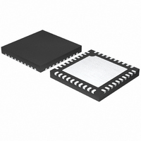
MAX1544ETL+ Maxim Integrated Products, MAX1544ETL+ Datasheet - Page 15

MAX1544ETL+
Manufacturer Part Number
MAX1544ETL+
Description
IC QUICK-PWM DUAL-PHASE 40-TQFN
Manufacturer
Maxim Integrated Products
Series
Quick-PWM™r
Datasheet
1.MAX1544ETLT.pdf
(42 pages)
Specifications of MAX1544ETL+
Applications
Controller, AMD Hammer
Voltage - Input
2 ~ 28 V
Number Of Outputs
1
Voltage - Output
0.68 ~ 1.55 V
Operating Temperature
-40°C ~ 100°C
Mounting Type
Surface Mount
Package / Case
40-TQFN Exposed Pad
Output Voltage
0.675 V to 1.55 V
Output Current
40 A
Input Voltage
4 V to 28 V
Mounting Style
SMD/SMT
Maximum Operating Temperature
+ 100 C
Minimum Operating Temperature
- 40 C
Lead Free Status / RoHS Status
Lead free / RoHS Compliant
20–24
PIN
14
15
16
17
18
19
25
26
27
28
29
30
31
OAIN+
D4–D0
NAME
PGND
OAIN-
VROK
BSTM
DHM
SKIP
OVP
LXM
DLM
V
CCI
______________________________________________________________________________________
FB
DD
AMD Hammer CPU Core Power Supplies
Dual-Phase, Quick-PWM Controller for
Current Balance Compensation. Connect a 470pF capacitor between CCI and FB. See the Current
Balance Compensation section.
Feedback Input. FB is internally connected to both the feedback input and the output of the voltage-
positioning op amp. See the Setting Voltage Positioning section to set the voltage-positioning gain.
Op Amp Inverting Input and Op Amp Disable Input. When using the internal op amp for additional
voltage-positioning gain, connect to the negative terminal of current-sense resistor through a resistor
as described in the Setting Voltage Positioning section. Connect OAIN- to V
The logic threshold to disable the op amp is approximately V
Op Amp Noninverting Input. When using the internal op amp for additional voltage-positioning gain,
connect to the positive terminal of current-sense resistor through a resistor as described in the Setting
Voltage Positioning section.
Pulse-Skipping Select Input. When pulse skipping, the controller blanks the VROK upper threshold:
3.3V or V
REF = Dual-phase pulse-skipping operation
GND = Single-phase pulse-skipping operation
Overvoltage Protection Enable Input. Connect OVP to V
protection. Connect OVP to GND to disable the output overvoltage fault protection. During normal
forced-PWM operation (SKIP = high), the controller detects an OVP fault if the output voltage exceeds
the set DAC voltage by more than 13% (min). During pulse-skipping operation (SKIP = REF or GND),
the controller detects an OVP fault if the output voltage exceeds the fixed 2V (typ) threshold. If an
overvoltage fault occurs, the controller is immediately shutdown and the output is discharged. See
the Fault Protection section.
Low-Voltage VID DAC Code Inputs. The D0–D4 inputs do not have internal pullups. These 1.0V logic
inputs are designed to interface directly with the CPU. In normal mode (Table 4, SUS = GND), the
output voltage is set by the VID code indicated by the logic-level voltages on D0-D4. In suspend
mode (Table 5, SUS = REF or high), the decoded state of the four-level S0–S1 inputs sets the output
voltage.
Open-Drain Power-Good Output. After output voltage transitions, except during power-up and power-
down, if OUT is in regulation then VROK is high impedance. The controller blanks VROK whenever
the slew rate control is active (output voltage transitions). VROK is forced low in shutdown. A pullup
resistor on VROK causes additional finite shutdown current. During power-up, VROK includes a 3ms
(min) delay after the output reaches the regulation voltage.
Main Boost Flying Capacitor Connection. An optional resistor in series with BSTM allows the DHM
pullup current to be adjusted.
Main Inductor Connection. LXM is the internal lower supply rail for the DHM high-side gate driver.
Main High-Side Gate-Driver Output. Swings LXM to BSTM.
M ai n Low - S i d e G ate- D r i ver O utp ut. D LM sw i ng s fr om P GN D to V
M AX 1544 p ow er s d ow n.
Supply Voltage Input for the DLM and DLS Gate Drivers. Connect to the system supply voltage (4.5V
to 5.5V). Bypass V
possible.
Power Ground. Ground connection for low-side gate drivers DLM and DLS.
CC
(high) = Dual-phase forced-PWM operation
DD
to PGND with a 2.2µF or greater ceramic capacitor as close to the IC as
FUNCTION
Pin Description (continued)
CC
to enable the output overvoltage fault
CC
D D
- 1V.
. D LM i s for ced hi g h after the
CC
to disable the op amp.
15


