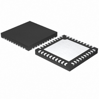
MAX1544ETL+ Maxim Integrated Products, MAX1544ETL+ Datasheet - Page 16

MAX1544ETL+
Manufacturer Part Number
MAX1544ETL+
Description
IC QUICK-PWM DUAL-PHASE 40-TQFN
Manufacturer
Maxim Integrated Products
Series
Quick-PWM™r
Datasheet
1.MAX1544ETLT.pdf
(42 pages)
Specifications of MAX1544ETL+
Applications
Controller, AMD Hammer
Voltage - Input
2 ~ 28 V
Number Of Outputs
1
Voltage - Output
0.68 ~ 1.55 V
Operating Temperature
-40°C ~ 100°C
Mounting Type
Surface Mount
Package / Case
40-TQFN Exposed Pad
Output Voltage
0.675 V to 1.55 V
Output Current
40 A
Input Voltage
4 V to 28 V
Mounting Style
SMD/SMT
Maximum Operating Temperature
+ 100 C
Minimum Operating Temperature
- 40 C
Lead Free Status / RoHS Status
Lead free / RoHS Compliant
Dual-Phase, Quick-PWM Controller for
AMD Hammer CPU Core Power Supplies
The two phases in the MAX1544 operate 180° out-of-
phase (SKIP = REF or high) to minimize input and output
filtering requirements, reduce electromagnetic interfer-
ence (EMI), and improve efficiency. This effectively low-
ers component count—reducing cost, board space, and
component power requirements—making the MAX1544
ideal for high-power, cost-sensitive applications.
Typically, switching regulators provide transfer power
using only one phase instead of dividing the power
among several phases. In these applications, the input
capacitors must support high-instantaneous current
requirements. The high-RMS ripple current can lower
efficiency due to I
capacitor’s effective series resistance (ESR). Therefore,
the system typically requires several low-ESR input
capacitors in parallel to minimize input voltage
ripple, to reduce ESR-related power losses, and to meet
the necessary RMS ripple current rating.
With the MAX1544, the controller shares the current
between two phases that operate 180° out-of-phase, so
the high-side MOSFETs never turn on simultaneously
during normal operation. The instantaneous input cur-
rent of either phase is effectively cut in half, resulting in
16
______________________________________________________________________________________
PIN
32
33
34
35
36
37
38
39
40
Dual 180° Out-of-Phase Operation
NAME
2
BSTS
CMN
DHS
CMP
CSN
CSP
DLS
LXS
R power loss associated with the input
V+
Detailed Description
S econd ar y Low - S i d e G ate- D r i ver O utp ut. D LS sw i ng s fr om P GN D to V
M AX 1544 p ow er s d ow n.
Secondary High-Side Gate-Driver Output. Swings LXS to BSTS.
Secondary Inductor Connection. LXS is the internal lower supply rail for the DHS high-side gate
driver.
Secondary Boost Flying Capacitor Connection. An optional resistor in series with BSTS allows the
DHS pullup current to be adjusted.
Battery Voltage-Sense Connection. Used only for PWM one-shot timing. DH_ on-time is inversely
proportional to input voltage over a range of 4V to 28V.
Main Inductor Positive Current-Sense Input
Main Inductor Negative Current-Sense Input
Secondary Inductor Positive Current-Sense Input
Secondary Inductor Negative Current-Sense Input
reduced input voltage ripple, ESR power loss, and RMS
ripple current (see the Input Capacitor Selection sec-
tion). As a result, the same performance can be
achieved with fewer or less-expensive input capacitors.
Table 1 lists component selection for standard multi-
phase selections and Table 2 is a list of component
suppliers.
When a transient occurs, the response time of the con-
troller depends on how quickly it can slew the inductor
current. Multiphase controllers that remain 180 degrees
out-of-phase when a transient occurs actually respond
slower than an equivalent single-phase controller. In
order to provide fast transient response, the MAX1544
supports a phase-overlap mode, which allows the dual
regulators to operate in-phase when heavy-load tran-
sients are detected, reducing the response time. After
either high-side MOSFET turns off, if the output voltage
does not exceed the regulation voltage when the mini-
mum off-time expires, the controller simultaneously
turns on both high-side MOSFETs during the next on-
time cycle. This maximizes the total inductor current
slew rate. The phases remain overlapped until the out-
put voltage exceeds the regulation voltage after the
minimum off-time expires.
FUNCTION
Pin Description (continued)
Transient Overlap Operation
D D
. D LS i s for ced hi g h after the


