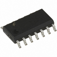
FAN1655MX Fairchild Semiconductor, FAN1655MX Datasheet - Page 5

FAN1655MX
Manufacturer Part Number
FAN1655MX
Description
IC REG LDO DDR BUS 3A 14SOIC
Manufacturer
Fairchild Semiconductor
Datasheet
1.FAN1655MPX.pdf
(9 pages)
Specifications of FAN1655MX
Applications
Controller, DDR
Voltage - Input
2.3 ~ 3.6 V
Number Of Outputs
1
Voltage - Output
1.1 ~ 1.8 V
Operating Temperature
0°C ~ 125°C
Mounting Type
Surface Mount
Package / Case
14-SOIC (3.9mm Width), 14-SOL
Polarity
Positive
Input Voltage Max
3.6 V
Output Voltage
1.15 V, 1.25 V, 1.35 V
Output Type
Selectable
Output Current
3 A
Load Regulation
40 mV
Maximum Power Dissipation
1.4 W
Maximum Operating Temperature
+ 125 C
Mounting Style
SMD/SMT
Minimum Operating Temperature
0 C
Reference Voltage
1.355 V
Lead Free Status / RoHS Status
Lead free / RoHS Compliant
Available stocks
Company
Part Number
Manufacturer
Quantity
Price
Company:
Part Number:
FAN1655MX
Manufacturer:
TOREX
Quantity:
3 000
Part Number:
FAN1655MX
Manufacturer:
FAIRCHILD/仙童
Quantity:
20 000
FAN1655 Rev. 1.1.5
Applications Information
Output Capacitor selection
The JEDEC specification for DDR termination requires
that VTT stay within ±40mV of VREF, which must track
VDDQ/2 within 1%. During the initial load transient, the
output capacitor keeps the output within spec. To stay
within the 40mV window, the “load step” due to the load
transient current dropping across the output capacitor’s
ESR should be kept to around 25mV: where ESR <
For example, to handle a 3A maximum load transient,
the ESR should be no greater than 8m . Furthermore,
the output capacitor must be able to hold the load in
spec while the regulator recovers (about 15µS). A mini-
mum value of 470µF is recommended.
The FAN1655 requires a minimum of 100µF of input
capacitance with a maximum ESR value of 100m
insure stability.
25
----- -
I
is given in m , and I is the maximum load current.
to
5
Power Dissipation and Derating
The maximum output current (sink or source) for a 1.25V
output is:
where P
is:
where T
and T
FAN1655 has an internal thermal limit at 150°C, which
defines T
at 88°C/W. Using equation 2, the maximum dissipation
at T
pation.
The e-TSSOP or MLP package, however, use the PCB
copper to cool the IC through the thermal pad on the
package bottom.
should be soldered to the PCB copper, with as much
copper area as possible surrounding it to cool the pack-
age. Thermal vias should be placed as close to the ther-
mal pad as possible to transfer heat to other layers of
copper on the PCB. With large areas of PCB copper for
heat sinking, a
achieved.
A
I
P
OUT MAX
A
= 25°C is 1.4W, which is its rated maximum dissi-
D MAX
is the operating ambient temperature.
J(MAX)
D(MAX)
J(MAX)
=
is the maximum die temperature of the IC
. For the SOIC-14 package,
is the maximum power dissipation which
=
T
--------------------------------- -
J MAX
P
--------------------- -
JA
For maximum dissipation, this pad
D MAX
1.25
of under 40°C/W can easily be
JA
–
T
A
www.fairchildsemi.com
JA
is given


