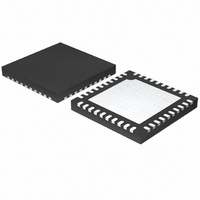
ISL6566ACRZ-T Intersil, ISL6566ACRZ-T Datasheet - Page 8

ISL6566ACRZ-T
Manufacturer Part Number
ISL6566ACRZ-T
Description
IC CTRLR PWM 3PHASE BUCK 40-QFN
Manufacturer
Intersil
Datasheet
1.ISL6566ACRZ.pdf
(28 pages)
Specifications of ISL6566ACRZ-T
Pwm Type
Voltage Mode
Number Of Outputs
1
Frequency - Max
1.5MHz
Duty Cycle
66.6%
Voltage - Supply
4.75 V ~ 12 V
Buck
Yes
Boost
No
Flyback
No
Inverting
No
Doubler
No
Divider
No
Cuk
No
Isolated
No
Operating Temperature
0°C ~ 70°C
Package / Case
40-VFQFN, 40-VFQFPN
Frequency-max
1.5MHz
Lead Free Status / RoHS Status
Lead free / RoHS Compliant
to smooth the voltage transition during Dynamic VID
operations.
OFS
The OFS pin provides a means to program a dc current for
generating an offset voltage across the resistor between FB
and VDIFF. The offset current is generated via an external
resistor and precision internal voltage references. The polarity
of the offset is selected by connecting the resistor to GND or
VCC. For no offset, the OFS pin should be left unconnected.
OCSET
This is the overcurrent set pin. Placing a resistor from OCSET
to ICOMP allows a 100µA current to flow out this pin,
producing a voltage reference. Internal circuitry compares the
voltage at OCSET to the voltage at ISUM, and if ISUM ever
exceeds OCSET, the overcurrent protection activates.
ISEN1, ISEN2 and ISEN3
These pins are used for balancing the channel currents by
sensing the current through each channel’s lower MOSFET
when it is conducting. Connect a resistor between the
ISEN1, ISEN2, and ISEN3 pins and their respective phase
node. This resistor sets a current proportional to the current
in the lower MOSFET during its conduction interval.
UGATE1 and UGATE2
Connect these pins to the corresponding upper MOSFET
gates. These pins are used to control the upper MOSFETs
and are monitored for shoot-through prevention purposes.
Maximum individual channel duty cycle is limited to 66%.
BOOT1 and BOOT2
These pins provide the bias voltage for the corresponding
upper MOSFET drives. Connect these pins to appropriately-
chosen external bootstrap capacitors. Internal bootstrap
diodes connected to the PVCC pins provide the necessary
bootstrap charge.
PHASE1 and PHASE2
Connect these pins to the sources of the upper MOSFETs.
These pins are the return path for the upper MOSFET
drives.
LGATE1 and LGATE2
These pins are used to control the lower MOSFETs. Connect
these pins to the corresponding lower MOSFETs’ gates.
PWM3
Pulse-width modulation output. Connect this pin to the PWM
input pin of an Intersil driver IC if 3-phase operation is
desired.
EN_PH3
This pin has two functions. First, a resistor divider connected
to this pin will provide a POR power up synch between the
on-chip and external driver. The resistor divider should be
8
ISL6566A
ISL6566A
designed so that when the POR-trip point of the external
driver is reached the voltage on this pin should be 1.220V.
The second function of this pin is disabling PWM3 for 2-
phase operation. This can be accomplished by connecting
this pin to a +5V supply.
PGOOD
During normal operation PGOOD indicates whether the
output voltage is within specified overvoltage and
undervoltage limits. If the output voltage exceeds these limits
or a reset event occurs (such as an overcurrent event),
PGOOD is pulled low. PGOOD is always low prior to the end
of soft-start.
Operation
Multi-Phase Power Conversion
Microprocessor load current profiles have changed to the
point that the advantages of multi-phase power conversion
are impossible to ignore. The technical challenges
associated with producing a single-phase converter that is
both cost-effective and thermally viable have forced a
change to the cost-saving approach of multi-phase. The
ISL6566A controller helps simplify implementation by
integrating vital functions and requiring minimal external
components. The block diagram on page 2 provides a top
level view of multi-phase power conversion using the
ISL6566A controller.
Interleaving
The switching of each channel in a multi-phase converter is
timed to be symmetrically out of phase with each of the other
channels. In a 3-phase converter, each channel switches 1/3
cycle after the previous channel and 1/3 cycle before the
following channel. As a result, the three-phase converter has
a combined ripple frequency three times greater than the
ripple frequency of any one phase. In addition, the peak-to-
peak amplitude of the combined inductor currents is reduced
in proportion to the number of phases (Equations 1 and 2).
FIGURE 1. PWM AND INDUCTOR-CURRENT WAVEFORMS
PWM1, 5V/DIV
IL1 + IL2 + IL3, 7A/DIV
FOR 3-PHASE CONVERTER
IL1, 7A/DIV
PWM3, 5V/DIV
1µs/DIV
IL3, 7A/DIV
PWM2, 5V/DIV
IL2, 7A/DIV
July 27, 2005
FN9200.2


