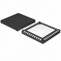
ISL6566ACRZ-T Intersil, ISL6566ACRZ-T Datasheet - Page 22

ISL6566ACRZ-T
Manufacturer Part Number
ISL6566ACRZ-T
Description
IC CTRLR PWM 3PHASE BUCK 40-QFN
Manufacturer
Intersil
Datasheet
1.ISL6566ACRZ.pdf
(28 pages)
Specifications of ISL6566ACRZ-T
Pwm Type
Voltage Mode
Number Of Outputs
1
Frequency - Max
1.5MHz
Duty Cycle
66.6%
Voltage - Supply
4.75 V ~ 12 V
Buck
Yes
Boost
No
Flyback
No
Inverting
No
Doubler
No
Divider
No
Cuk
No
Isolated
No
Operating Temperature
0°C ~ 70°C
Package / Case
40-VFQFN, 40-VFQFPN
Frequency-max
1.5MHz
Lead Free Status / RoHS Status
Lead free / RoHS Compliant
Due to errors in the inductance or DCR it may be necessary
to adjust the value of R
correctly. The effects of time constant mismatch can be seen
in the form of droop overshoot or undershoot during the
initial load transient spike, as shown in Figure 19. Follow the
steps below to ensure the R-C and inductor L/DCR time
constants are matched accurately.
After choosing a new value for R
necessary to adjust the value of R
load droop voltage. Use Equation 27 to obtain the new value
for R
1. Capture a transient event with the oscilloscope set to
2. Record ∆V1 and ∆V2 as shown in Figure 19.
3. Select a new value, R
4. Replace R
To External Driver
about L/DCR/2 (sec/div). For example, with L = 1µH and
DCR = 1mΩ, set the oscilloscope to 500µs/div.
resistor based on the original value, R
following equation.
the error is corrected. Repeat the procedure if necessary.
R
S
PHASE Pin
COMP 2
V
.
DROOP
ISL6566A
FIGURE 18. DCR SENSING CONFIGURATION
+
-
PHASE2
PHASE1
,
ICOMP
ISUM
PHASE3
IREF
=
COMP
R
COMP 1
with the new value and check to see that
COMP
,
(optional)
R
COMP,2
⋅
S
∆
----------
∆
C
V
V
22
R
COMP
1
2
to match the time constants
S
COMP
, for the time constant
R
S
S
to obtain the desired full
R
I
I
I
L2
L1
COMP
L3
INDUCTOR
, it will most likely be
INDUCTOR
INDUCTOR
L
L
L
V
COMP,1
L
(s)
DCR
DCR
DCR
-
, using the
(EQ. 28)
C
I
OUT
OUT
ISL6566A
Compensation
The two opposing goals of compensating the voltage
regulator are stability and speed.
The load-line regulated converter behaves in a similar
manner to a peak current mode controller because the two
poles at the output filter L-C resonant frequency split with the
introduction of current information into the control loop. The
final location of these poles is determined by the system
function, the gain of the current signal, and the value of the
compensation components, R
Since the system poles and zero are affected by the values
of the components that are meant to compensate them, the
solution to the system equation becomes fairly complicated.
Fortunately, there is a simple approximation that comes very
close to an optimal solution. Treating the system as though it
were a voltage-mode regulator, by compensating the L-C
poles and the ESR zero of the voltage mode approximation,
yields a solution that is always stable with very close to ideal
transient performance.
Select a target bandwidth for the compensated system, f
The target bandwidth must be large enough to assure
adequate transient performance, but smaller than 1/3 of the
FIGURE 20. COMPENSATION CONFIGURATION FOR
FIGURE 19. TIME CONSTANT MISMATCH BEHAVIOR
∆V
1
R
FB
LOAD-LINE REGULATED ISL6566A CIRCUIT
R
C
C
2
C
(OPTIONAL)
C
C
and C
COMP
VDIFF
FB
C
.
∆V
∆I
2
ISL6566A
July 27, 2005
V
I
TRAN
OUT
FN9200.2
0
.


