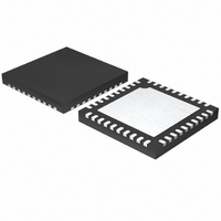
ISL6566ACRZ-T Intersil, ISL6566ACRZ-T Datasheet - Page 20

ISL6566ACRZ-T
Manufacturer Part Number
ISL6566ACRZ-T
Description
IC CTRLR PWM 3PHASE BUCK 40-QFN
Manufacturer
Intersil
Datasheet
1.ISL6566ACRZ.pdf
(28 pages)
Specifications of ISL6566ACRZ-T
Pwm Type
Voltage Mode
Number Of Outputs
1
Frequency - Max
1.5MHz
Duty Cycle
66.6%
Voltage - Supply
4.75 V ~ 12 V
Buck
Yes
Boost
No
Flyback
No
Inverting
No
Doubler
No
Divider
No
Cuk
No
Isolated
No
Operating Temperature
0°C ~ 70°C
Package / Case
40-VFQFN, 40-VFQFPN
Frequency-max
1.5MHz
Lead Free Status / RoHS Status
Lead free / RoHS Compliant
through the upper MOSFET across VIN. The power
dissipated as a result is P
Finally, the resistive part of the upper MOSFET is given in
Equation 20 as P
The total power dissipated by the upper MOSFET at full load
can now be approximated as the summation of the results
from Equations 17, 18, 19 and 20. Since the power
equations depend on MOSFET parameters, choosing the
correct MOSFETs can be an iterative process involving
repetitive solutions to the loss equations for different
MOSFETs and different switching frequencies.
Package Power Dissipation
When choosing MOSFETs it is important to consider the
amount of power being dissipated in the integrated drivers
located in the controller. Since there are a total of three
drivers in the controller package, the total power dissipated
by all three drivers must be less than the maximum
allowable power dissipation for the QFN package.
Calculating the power dissipation in the drivers for a desired
application is critical to ensure safe operation. Exceeding the
maximum allowable power dissipation level will push the IC
beyond the maximum recommended operating junction
temperature of 125°C. The maximum allowable IC power
dissipation for the 6x6 QFN package is approximately 4W at
room temperature. See Layout Considerations paragraph for
thermal transfer improvement suggestions.
When designing the ISL6566A into an application, it is
recommended that the following calculation is used to
ensure safe operation at the desired frequency for the
selected MOSFETs. The total gate drive power losses,
P
integrated driver’s internal circuitry and their corresponding
average driver current can be estimated with Equations 21
and 22, respectively.
P
P
P
P
P
Qg_TOT
Qg_Q2
UP 3 ,
UP 4 ,
Qg_Q1
Qg_TOT
≈
=
r
DS ON
=
=
V
, due to the gate charge of MOSFETs and the
=
IN
Q
3
-- - Q
2
(
P
G2
Q
•
Qg_Q1
rr
)
•
G1
f
S
PVCC
UP,4
I
----- -
N
M
•
+
PVCC
2
.
P
d
Qg_Q2
+
•
F
I
--------- -
UP,3
PP
12
SW
•
2
F
20
SW
+
•
.
N
I
Q
Q2
•
•
N
VCC
•
Q1
N
PHASE
•
N
PHASE
(EQ. 21)
(EQ. 19)
(EQ. 20)
ISL6566A
In Equations 21 and 22, P
power loss and P
loss; the gate charge (Q
particular gate to source drive voltage PVCC in the
corresponding MOSFET data sheet; I
quiescent current with no load at both drive outputs; N
and N
phase, respectively; N
being controlled by the internal ISL6566A drivers (can not be
greater then 2). The I
of the controller without capacitive load and is typically
75mW at 300kHz.
The total gate drive power losses are dissipated among the
resistive components along the transition path and in the
bootstrap diode. The portion of the total power dissipated in
the controller itself is the power dissipated in the upper drive
path resistance, P
P
power will be dissipated by the external gate resistors (R
and R
the MOSFETs. Figures 15 and 16 show the typical upper
and lower gate drives turn-on transition path. The total power
PVCC
I
DR
DR_UP
FIGURE 16. TYPICAL LOWER-GATE DRIVE TURN-ON PATH
FIGURE 15. TYPICAL UPPER-GATE DRIVE TURN-ON PATH
PVCC
=
Q2
G2
PHASE
3
-- - Q
2
, and in the boot strap diode, P
) and the internal gate resistors (R
R
•
are the number of upper and lower MOSFETs per
R
BOOT
LO2
HI2
R
R
G1
LO1
HI1
•
N
Qg_Q2
DR_UP
Q1
LGATE
+
Q*
UGATE
PHASE
Q
VCC product is the quiescent power
G1
G2
is the total lower gate drive power
, the lower drive path resistance,
Qg_Q1
and Q
•
N
R
is the number of active phases
Q2
G2
R
G
G1
is the total upper gate drive
G2
G
•
R
C
N
) is defined at the
GI2
R
GD
C
PHASE
Q
C
GI1
GD
BOOT
GS
C
is the driver total
GS
GI1
S
. The rest of the
•
S
F
and R
SW
D
D
Q2
+
C
July 27, 2005
Q1
DS
I
C
(EQ. 22)
Q
GI2
FN9200.2
DS
Q1
) of
G1


