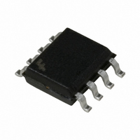
FAN7554DTF Fairchild Semiconductor, FAN7554DTF Datasheet - Page 11

FAN7554DTF
Manufacturer Part Number
FAN7554DTF
Description
IC CTRLR PWM CURRENT MODE 8SOIC
Manufacturer
Fairchild Semiconductor
Datasheet
1.FAN7554DTF.pdf
(22 pages)
Specifications of FAN7554DTF
Pwm Type
Current Mode
Number Of Outputs
1
Frequency - Max
500kHz
Duty Cycle
98%
Voltage - Supply
9 V ~ 30 V
Buck
No
Boost
No
Flyback
Yes
Inverting
No
Doubler
No
Divider
No
Cuk
No
Isolated
Yes
Operating Temperature
-25°C ~ 85°C
Package / Case
8-SOIC (3.9mm Width)
Frequency-max
500kHz
Output Current
1 A
Switching Frequency
500 KHz
Mounting Style
SMD/SMT
Maximum Operating Temperature
+ 85 C
Minimum Operating Temperature
- 25 C
Lead Free Status / RoHS Status
Lead free / RoHS Compliant
Other names
FAN7554DTFTR
FAN7554DTF_NL
FAN7554DTF_NLTR
FAN7554DTF_NLTR
FAN7554DTF_NL
FAN7554DTF_NLTR
FAN7554DTF_NLTR
Available stocks
Company
Part Number
Manufacturer
Quantity
Price
Part Number:
FAN7554DTF
Manufacturer:
FAIRCHILD/仙童
Quantity:
20 000
Gate Driver
The gate drive circuit has the totem-pole output configuration. The output has 1A peak current and 200mA average current
drive ability.
ON/OFF Control
The FAN7554 is able to use the feedback pin for ON/OFF control by placing NPN transistor between the cathode of the
KA431 and ground as shown in figure 19. When the transistor turns on, the current flows through the photo diode and
saturates the photo transistor. As a result, the feedback voltage is dropped to zero. When the feedback voltage is below 0.3V,
the soft start voltage starts to discharge by connecting the internal resistor 1k in parallel with the external capacitor Cs. When
the soft start voltage becomes less than 1.5V, all the blocks in the FAN7554 are turned off , with the exceptions of the UVLO
block and ON/OFF control block. The operation current is about 200uA. So the stand-by power is reduced and SMPS
efficiency is improved. When the feedback voltage exceeds 0.3V, the FAN7554 normally operates by turning on Vref block.
6V
6V
3V
3V
Vfb
Vfb
t1
t1
Slope (dv/dt) = 5uA / Cfb
Slope (dv/dt) = 5uA / Cfb
Shutdown
Shutdown
Shutdown
Clock
Clock
Clock
Q
Q
Q
Figure 17-B . Delayed Shutdown & Feedback Waveform
Figure 18. Gate Drive Circuit
FAN7554
FAN7554
FAN7554
7
7
7
t2
t2
6
6
6
OUT
OUT
OUT
Shutdown start point
Shutdown start point
DRAIN
DRAIN
FAN7554
t
t
11


