SE97BTP,547 NXP Semiconductors, SE97BTP,547 Datasheet - Page 20
SE97BTP,547
Manufacturer Part Number
SE97BTP,547
Description
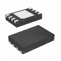
IC TEMP SENSOR DIMM 8HWSON
Manufacturer
NXP Semiconductors
Datasheet
1.SE97BTP547.pdf
(53 pages)
Specifications of SE97BTP,547
Package / Case
8-WSON (Exposed Pad), 8-HWSON
Function
Temp Monitoring System (Sensor)
Topology
ADC (Sigma Delta), Comparator, Register Bank
Sensor Type
Internal
Sensing Temperature
-40°C ~ 125°C
Output Type
I²C™/SMBus™
Output Alarm
Yes
Output Fan
Yes
Voltage - Supply
3 V ~ 3.6 V
Operating Temperature
-40°C ~ 125°C
Mounting Type
Surface Mount
Temperature Threshold
+ 150 C
Full Temp Accuracy
2 C
Digital Output - Bus Interface
I2C
Digital Output - Number Of Bits
11 bit
Supply Voltage (max)
3.6 V
Supply Voltage (min)
3 V
Description/function
Temperature Sensor
Maximum Operating Temperature
+ 125 C
Minimum Operating Temperature
- 40 C
Lead Free Status / RoHS Status
Lead free / RoHS Compliant
Lead Free Status / RoHS Status
Lead free / RoHS Compliant, Lead free / RoHS Compliant
Other names
568-5055-2


NXP Semiconductors
SE97B_1
Product data sheet
7.10.3.1 Current address read
7.10.3.2 Selective read
7.10.3 Read operations
In Standby mode, the SE97B internal address counter points to the data byte immediately
following the last byte accessed by a previous operation. If the ‘previous’ byte was the last
byte in memory, then the address counter will point to the first memory byte, and so on. If
the SE97B decodes a slave address with a ‘1’ in the R/W bit position
issue an Acknowledge in the ninth clock cycle and will then transmit the data byte being
pointed at by the address counter. The master can then stop further transmission by
issuing a No Acknowledge on the ninth bit then followed by a STOP condition.
The read operation can also be started at an address different from the one stored in the
address counter. The address counter can be ‘initialized’ by performing a ‘dummy’ write
operation
R/W bit set to ‘0’) and the desired byte address. Instead of following-up with data, the
master then issues a second START, followed by the ‘Current Address Read’ sequence,
as described in
Fig 15. Current address read timing
Fig 16. Selective read timing
(Figure
SDA
SDA
Section
START condition
START condition
START condition
S
S
S
16). The START condition is followed by the slave address (with the
1
1
1
slave address (memory)
slave address (memory)
slave address (memory)
Rev. 01 — 27 January 2010
0
0
0
7.10.3.1.
1
1
1
0
0
0
DDR memory module temp sensor with integrated SPD
A2 A1 A0
A2 A1 A0
A2 A1 A0
R/W acknowledge
R/W acknowledge
R/W acknowledge
0
1
1
A
from slave
A
from slave
A
from slave
data from memory
data from memory
word address
no acknowledge
no acknowledge
acknowledge
from master
from master
STOP condition
STOP condition
from slave
(Figure
002aac901
002aab251
© NXP B.V. 2010. All rights reserved.
A
A
A
SE97B
P
P
15), it will
20 of 53
Related parts for SE97BTP,547
Image
Part Number
Description
Manufacturer
Datasheet
Request
R

Part Number:
Description:
DDR memory module temp sensor with integrated SPD
Manufacturer:
NXP [NXP Semiconductors]
Datasheet:
Part Number:
Description:
DDR memory module temp sensor with integrated SPD, 3.3 V
Manufacturer:
NXP [NXP Semiconductors]
Datasheet:

Part Number:
Description:
Se97 Memory Module Temp Sensor With Integrated Spd
Manufacturer:
NXP Semiconductors
Datasheet:
Part Number:
Description:
NXP Semiconductors designed the LPC2420/2460 microcontroller around a 16-bit/32-bitARM7TDMI-S CPU core with real-time debug interfaces that include both JTAG andembedded trace
Manufacturer:
NXP Semiconductors
Datasheet:

Part Number:
Description:
NXP Semiconductors designed the LPC2458 microcontroller around a 16-bit/32-bitARM7TDMI-S CPU core with real-time debug interfaces that include both JTAG andembedded trace
Manufacturer:
NXP Semiconductors
Datasheet:
Part Number:
Description:
NXP Semiconductors designed the LPC2468 microcontroller around a 16-bit/32-bitARM7TDMI-S CPU core with real-time debug interfaces that include both JTAG andembedded trace
Manufacturer:
NXP Semiconductors
Datasheet:
Part Number:
Description:
NXP Semiconductors designed the LPC2470 microcontroller, powered by theARM7TDMI-S core, to be a highly integrated microcontroller for a wide range ofapplications that require advanced communications and high quality graphic displays
Manufacturer:
NXP Semiconductors
Datasheet:
Part Number:
Description:
NXP Semiconductors designed the LPC2478 microcontroller, powered by theARM7TDMI-S core, to be a highly integrated microcontroller for a wide range ofapplications that require advanced communications and high quality graphic displays
Manufacturer:
NXP Semiconductors
Datasheet:
Part Number:
Description:
The Philips Semiconductors XA (eXtended Architecture) family of 16-bit single-chip microcontrollers is powerful enough to easily handle the requirements of high performance embedded applications, yet inexpensive enough to compete in the market for hi
Manufacturer:
NXP Semiconductors
Datasheet:
Part Number:
Description:
The XA-S3 device is a member of Philips Semiconductors? XA(eXtended Architecture) family of high performance 16-bitsingle-chip microcontrollers
Manufacturer:
NXP Semiconductors
Datasheet:

Part Number:
Description:
The NXP BlueStreak LH75401/LH75411 family consists of two low-cost 16/32-bit System-on-Chip (SoC) devices
Manufacturer:
NXP Semiconductors
Datasheet:
Part Number:
Description:
The NXP LPC3130/3131 combine an 180 MHz ARM926EJ-S CPU core, high-speed USB2
Manufacturer:
NXP Semiconductors
Datasheet:
Part Number:
Description:
The NXP LPC3141 combine a 270 MHz ARM926EJ-S CPU core, High-speed USB 2
Manufacturer:
NXP Semiconductors
Part Number:
Description:
The NXP LPC3143 combine a 270 MHz ARM926EJ-S CPU core, High-speed USB 2
Manufacturer:
NXP Semiconductors