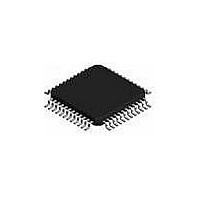
L6740L STMicroelectronics, L6740L Datasheet - Page 23

L6740L
Manufacturer Part Number
L6740L
Description
IC HYBRID CONTROLLERS 48TQFP
Manufacturer
STMicroelectronics
Datasheet
1.L6740LTR.pdf
(44 pages)
Specifications of L6740L
Applications
Hybrid Controllers
Voltage - Supply
9 V ~ 15 V
Current - Supply
20mA
Operating Temperature
0°C ~ 125°C
Mounting Type
Surface Mount
Package / Case
48-TQFP Exposed Pad, 48-eTQFP, 48-HTQFP, 48-VQFP
Number Of Outputs
2
Output Current
170 A
Input Voltage
13.2 V
Mounting Style
SMD/SMT
Maximum Operating Temperature
+ 125 C
Minimum Operating Temperature
0 C
Hybrid Controller
compatible with PVI and SVI CPUs
Dual Controller
2 to 4 scalable phases for CPU CORE, 1 phase for NB
Dual Over-current Protection
Average and per-phase
Lead Free Status / RoHS Status
Lead free / RoHS Compliant
Voltage - Input
-
Lead Free Status / Rohs Status
Lead free / RoHS Compliant
Available stocks
Company
Part Number
Manufacturer
Quantity
Price
Part Number:
L6740L
Manufacturer:
ST
Quantity:
20 000
Part Number:
L6740LTR
Manufacturer:
ST
Quantity:
20 000
L6740L
6
Output voltage positioning
Output voltage positioning is performed by selecting the controller operative-mode (SVI, PVI
and V_FIX) and by programming the droop function and offset to the reference of both the
sections (See
monitoring the voltage drop across the low-side MOSFET for NB section or DCR Inductors
for CORE section. The current (I
NB_DROOP pin, directly proportional to the read current, causes the related section output
voltage to vary according to the external R
load-line effect. The current (I
sunk from the FB / NB_FB pins causing the output voltage to be offset according to the
resistance R
L6740L embeds a dual remote-sense buffer to sense remotely the regulated voltage of each
section without any additional external components. In this way, the output voltage
programmed is regulated compensating for board and socket losses. Keeping the sense
traces parallel and guarded by a power plane results in common mode coupling for any
picked-up noise.
Both DROOP and OFFSET function can be disabled: see
details about CORE section and
case DROOP effect is not desired, the current information sourced from the DROOP pin
may be used to implement a Load Indicator as reported in
Figure 9.
1.2V
1.2V
FB
Voltage positioning
Figure
/ R
NB_OS
FB_NB
OS
9). The controller reads the current delivered by each section by
R
R
OS
OS_NB
NB_DROOP
connected.
DROOP
OS
DROOP
Section 6.6
/ I
R
OS_NB
FB_COMP_NB
R
FB_COMP
NB_FB
/ I
FB
) programmed through the OS / NB_OS pins is
DROOP_NB
FB
and
CORE_REFERENCE
/ R
R
NB_REFERENCE
R
R
FB_NB
R
F_NB
FB
FB_NB
F
Section 6.7
NB_COMP
) sourced from the DROOP /
C
COMP
C
F_NB
F
resistor so implementing the desired
Section 6.3
Section 6.3
CORE Protection
for details about NB section. In
NB_VSEN
Monitor
VSEN
Output voltage positioning
NB Protection
Monitor
and
and
FBG
NB_FBG
Section 6.4
Section
from DAC...
from DAC...
To VDD_CORE
(Remote Sense)
(Remote Sense)
To VDD_NB
6.6.
for
23/44


