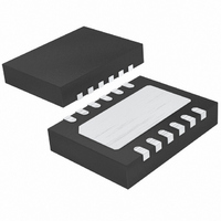
LTC2923CDE#PBF Linear Technology, LTC2923CDE#PBF Datasheet - Page 5

LTC2923CDE#PBF
Manufacturer Part Number
LTC2923CDE#PBF
Description
IC POWER SUPPLY CONTROLLER 12DFN
Manufacturer
Linear Technology
Datasheet
1.LTC2923CDEPBF.pdf
(20 pages)
Specifications of LTC2923CDE#PBF
Applications
Power Supply Controller
Voltage - Supply
2.9 V ~ 5.5 V
Operating Temperature
0°C ~ 70°C
Mounting Type
Surface Mount
Package / Case
12-DFN
Lead Free Status / RoHS Status
Lead free / RoHS Compliant
Current - Supply
-
Voltage - Input
-
Lead Free Status / Rohs Status
Compliant
Available stocks
Company
Part Number
Manufacturer
Quantity
Price
PI FU CTIO S
V
supply input range is 2.9V to 5.5V. An undervoltage
lockout circuit resets the part when the supply is below
2.5V. V
capacitor.
ON (Pin 2): On Control Input. The ON pin has a threshold
of 1.23V with 75mV of hysteresis. An active high will cause
10µA to flow from the GATE pin, ramping up the supplies.
An active low pulls 10µA from the GATE pin, ramping the
supplies down. Pulling the ON pin below 0.4V resets the
electronic circuit breaker in the LTC2923. If a resistive
divider connected to V
will automatically start up when V
TRACK1, TRACK2 (Pins 3, 4): Tracking Control Input. A
resistive voltage divider between RAMPBUF and TRACKx
determines the tracking profile of a slave supply (see
Applications Information). TRACKx pulls up to 0.8V and
the current supplied at TRACKx is mirrored at FBx. TRACKx
is capable of supplying at least 1mA when V
Because a TRACKx pin is capable of supplying up to 30mA
under short-circuit conditions, avoid connecting TRACKx
to GND for extended periods. Limit the capacitance at each
TRACKx pin to less than 25pF. Float the TRACKx pins if
unused.
RAMPBUF (Pin 5): Ramp Buffer Output. Provides a low
impedance buffered version of the signal on the RAMP pin.
This buffered output drives the resistive dividers that
connect to the TRACKx pins. Limit the capacitance at the
RAMPBUF pin to less than 100pF.
GND (Pins 6, 13): Circuit Ground.
FB1, FB2 (Pins 8, 7): Feedback Control Output. FBx pulls
up on the feedback node of slave supplies. Tracking is
achieved by mirroring the current from TRACKx into FBx.
If the appropriate resistive divider connects RAMPBUF
and TRACKx, the FBx current will force OUTx to track
RAMP. To prevent damage to the slave supply, the FBx pin
will not force the slave’s feedback node above 1.7V. In
addition, it will not actively sink current from this node
even when the LTC2923 is unpowered. Float the FB pins if
unused.
CC
U
(Pin 1): Positive Supply Input Pin. The operating
CC
U
should be bypassed to GND with a 0.1µF
U
CC
drives the ON pin, the supplies
MS/DE Packages
CC
is fully powered.
CC
= 2.9V.
GATE (Pin 9/Pin 11): Gate Drive for External N-Channel
FET. When the ON pin is high, an internal 10µA current
source charges the gate of the external N-channel MOS-
FET. A capacitor connected from GATE to GND sets the
ramp rate. An internal charge pump guarantees that GATE
will pull up to 5V above V
N-channel FETs are fully enhanced. When the ON pin is
pulled low, the GATE pin is pulled to GND with a 10µA
current source. Under a short-circuit condition, the elec-
tronic circuit breaker in the LTC2923 pulls the GATE low
immediately with 20mA. Tie GATE to GND if unused. It is
a good practice to add a 10Ω resistor between this
capacitor and the FET’s gate to prevent high frequency FET
oscillations.
RAMP (Pin 10/Pin 12): Ramp Buffer Input. When the
RAMP pin is connected to the source of the external
N-channel FET, the slave supplies track the FET’s source
as it ramps up and down. If the GATE is fully enhanced
(GATE > RAMP + 4.9V) and (V
indicates a shorted output, then the electronic circuit
breaker trips and GATE quickly pulls low with 20mA. The
GATE will not ramp up again until ON is pulled below 0.4V
and then above 1.23V. Alternatively, when no external FET
is used, the RAMP pin can be tied directly to the GATE pin.
In this configuration, the supplies track the capacitor on
the GATE pin as it is charged and discharged by the 10µA
current source controlled by the ON pin. RAMP must not
be driven above V
SDO (Pin 9, DE Package Only): Slave Supply Shutdown
Output. SDO is an open-drain output that holds the shut-
down (RUN/SS) pins of the slave supplies low until the ON
pin is pulled above 1.23V. If the slave supply is capable of
operating with an input supply that is lower than the
LTC2923’s minimum operating voltage of 2.9V, the SDO
pin can be used to hold off the slave supplies. SDO will be
pulled low again when RAMP < 100mV and ON < 1.23V.
STATUS (Pin 10, DE Package Only): Power Good Status
Indicator. The STATUS pin is an open-drain output that
pulls low until GATE has been fully charged at which time
all supplies will have reached their final operating voltage.
CC
(except by the GATE pin).
CC
ensuring that logic level
CC
– RAMP > 200mV)
LTC2923
2923fa
5


