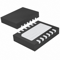
LTC2923CDE#PBF Linear Technology, LTC2923CDE#PBF Datasheet - Page 17

LTC2923CDE#PBF
Manufacturer Part Number
LTC2923CDE#PBF
Description
IC POWER SUPPLY CONTROLLER 12DFN
Manufacturer
Linear Technology
Datasheet
1.LTC2923CDEPBF.pdf
(20 pages)
Specifications of LTC2923CDE#PBF
Applications
Power Supply Controller
Voltage - Supply
2.9 V ~ 5.5 V
Operating Temperature
0°C ~ 70°C
Mounting Type
Surface Mount
Package / Case
12-DFN
Lead Free Status / RoHS Status
Lead free / RoHS Compliant
Current - Supply
-
Voltage - Input
-
Lead Free Status / Rohs Status
Compliant
Available stocks
Company
Part Number
Manufacturer
Quantity
Price
APPLICATIO S I FOR ATIO
MASTER
SLAVE2
SLAVE1
1V/DIV
1V/DIV
Figure 19. Power Supply Start-Ups Delayed
Figure 18. Weak Resistive Load
Figure 20. ON Pin Delayed
U
U
1ms/DIV
1ms/DIV
1ms/DIV
W
2923 F20
2923 F18
2923 F19
U
MASTER
SLAVE1
SLAVE2
ON
MASTER
SLAVE1
SLAVE2
ON
1V/DIV
Layout Considerations
Be sure to place a 0.1µF bypass capacitor as near as
possible to the supply pin of the LTC2923. A 10Ω resistor
located near the FET and connected between the FET’s
gate and the external C
This will almost assuredly eliminate the troublesome high
frequency oscillations that can occur due to the FET
interacting with PCB parasitics.
To minimize the noise on the slave supplies’ outputs, keep
the traces connecting the FBx pins of the LTC2923 and the
feedback nodes of the slave supplies as short as possible.
In addition, do not route those traces next to signals with
fast transition times. In some circumstances it might be
advantageous to add a resistor near the feedback node of
the slave supply in series with the FBx pin of the LTC2923.
This resistor must not exceed:
This resistor is most effective if there is already a capacitor
at the feedback node of the slave supply (often a compen-
sation component). Increasing the capacitance on a slave
supply’s feedback node will further improve the noise
immunity, but could affect the stability and transient
response of the supply.
R
SERIES
V
CC
=
V
CC
1 5
Figure 21. Layout Considerations
LTC2923
.
0.1µF
FET
I
V V
MAX
RAMP
GATE
GND
–
FB1
OUT
FB
GATE
10Ω
=
MINIMIZE
LENGTH
⎛
⎜
⎝
TRACE
capacitor is recommended.
1 5
V
.
FB
V
R
SERIES
–
C
1
GATE
⎞
⎟
⎠
(
LTC2923
R
R
2923 F21
FA
FA
FB
DC/DC
||
R
FB
R
OUT
FB
)
17
2923fa


