IR3505ZMTRPBF International Rectifier, IR3505ZMTRPBF Datasheet - Page 16
IR3505ZMTRPBF
Manufacturer Part Number
IR3505ZMTRPBF
Description
IC XPHASE3 CTLR 2.5A 16-MLPQ
Manufacturer
International Rectifier
Series
XPhase3™r
Datasheet
1.IR3505ZMTRPBF.pdf
(20 pages)
Specifications of IR3505ZMTRPBF
Package / Case
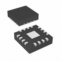
16-MLPQ
Mounting Type
Surface Mount
Current - Supply
3mA
Voltage - Supply
8 V ~ 16 V
Operating Temperature
0°C ~ 125°C
Applications
Processor
Supply Voltage Range
4.75V To 7.5V, 8V To 16V
Operating Temperature Range
0°C To +125°C
Digital Ic Case Style
MLPQ
No. Of Pins
16
Termination Type
SMD
Function
For High Performance CPUs And ASICs
Rohs Compliant
Yes
Filter Terminals
SMD
Controller Type
XPhase
Package
16-Lead MLPQ
Circuit
X-Phase Phase IC
Iout (a)
2.5A Gate Driver
Pbf
PbF Option Available
Lead Free Status / RoHS Status
Lead free / RoHS Compliant
Available stocks
Company
Part Number
Manufacturer
Quantity
Price

Part Number:
IR3505ZMTRPBF
Manufacturer:
IR
Quantity:
20 000


LAYOUT GUIDELINES
The following layout guidelines are recommended to reduce the parasitic inductance and resistance of the
PCB layout, therefore minimizing the noise coupled to the IC.
• Dedicate at least one middle layer for a ground plane.
• Separate analog bus (EAIN, DACIN, and ISHARE) from digital bus (CLKIN, PHSIN, and PHSOUT) to
• Connect PGND and LGND pins to the ground plane through vias.
• Place current sense resistors and capacitors (R
• Place the decoupling capacitor C
• Place the phase IC as close as possible to the MOSFETs to reduce the parasitic resistance and
• Place the input ceramic capacitors close to the drain of top MOSFET and the source of bottom MOSFET.
• There are two switching power loops. One loop includes the input capacitors, top MOSFET, inductor,
reduce the noise coupling.
the inductor current sense wires, but separate the two wires by ground polygon or route as a differential
pair. The wire from the inductor terminal to CSIN- should not cross over the fast transition nodes, i.e.
switching nodes, gate drive outputs and bootstrap nodes.
inductance of the gate drive paths.
Use a combination of different packages of ceramic capacitors.
output capacitors and the load; another loop consists of bottom MOSFET, inductor, output capacitors and
the load. Route the switching power paths using wide and short traces or polygons; use multiple vias for
connections between layers.
Page 16 of 20
VCCL
as close as possible to the VCCL pin.
CS
and C
CS
) close to phase IC. Use Kelvin connection for
March 17, 2009
IR3505Z
Related parts for IR3505ZMTRPBF
Image
Part Number
Description
Manufacturer
Datasheet
Request
R

Part Number:
Description:
Xphase3 Phase Ic
Manufacturer:
International Rectifier Corp.
Datasheet:

Part Number:
Description:
Receiver Pre-amp Module
Manufacturer:
ETC
Datasheet:
Part Number:
Description:
SCHOTTKY RECTIFIER
Manufacturer:
International Rectifier Corp.
Datasheet:
Part Number:
Description:
SCHOTTKY RECTIFIER
Manufacturer:
International Rectifier Corp.
Datasheet:
Part Number:
Description:
SCHOTTKY RECTIFIER
Manufacturer:
International Rectifier Corp.
Datasheet:
Part Number:
Description:
SCHOTTKY RECTIFIER
Manufacturer:
International Rectifier Corp.
Datasheet:
Part Number:
Description:
SCHOTTKY RECTIFIER
Manufacturer:
International Rectifier Corp.
Datasheet:
Part Number:
Description:
SCHOTTKY RECTIFIER
Manufacturer:
International Rectifier Corp.
Datasheet:
Part Number:
Description:
SCHOTTKY RECTIFIER
Manufacturer:
International Rectifier Corp.
Datasheet:
Part Number:
Description:
SCHOTTKY RECTIFIER
Manufacturer:
International Rectifier Corp.
Datasheet:
Part Number:
Description:
SCHOTTKY RECTIFIER
Manufacturer:
International Rectifier Corp.
Datasheet:
Part Number:
Description:
SCHOTTKY RECTIFIER
Manufacturer:
International Rectifier Corp.
Datasheet:
Part Number:
Description:
SCHOTTKY RECTIFIER
Manufacturer:
International Rectifier Corp.
Datasheet:
Part Number:
Description:
SCHOTTKY RECTIFIER
Manufacturer:
International Rectifier Corp.
Datasheet:
Part Number:
Description:
SCHOTTKY RECTIFIER
Manufacturer:
International Rectifier Corp.
Datasheet: