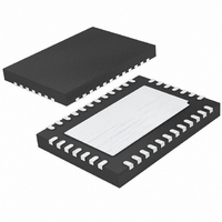
LTC3576EUFE#PBF Linear Technology, LTC3576EUFE#PBF Datasheet - Page 6

LTC3576EUFE#PBF
Manufacturer Part Number
LTC3576EUFE#PBF
Description
IC POWER MANAGER W/USB OTG 38QFN
Manufacturer
Linear Technology
Datasheet
1.LTC3576EUFEPBF.pdf
(48 pages)
Specifications of LTC3576EUFE#PBF
Applications
Handheld/Mobile Devices
Voltage - Supply
4.35 V ~ 5.5 V
Operating Temperature
-40°C ~ 85°C
Mounting Type
Surface Mount
Package / Case
38-QFN
Lead Free Status / RoHS Status
Lead free / RoHS Compliant
Current - Supply
-
Available stocks
Company
Part Number
Manufacturer
Quantity
Price
LTC3576/LTC3576-1
ELECTRICAL CHARACTERISTICS
Note 1: Stresses beyond those listed under Absolute Maximum Ratings
may cause permanent damage to the device. Exposure to any Absolute
Maximum Rating condition for extended periods may affect device
reliability and lifetime.
Note 2: The LTC3576E/LTC3576E-1 are guaranteed to meet performance
specifi cations from 0°C to 85°C. Specifi cations over the –40°C to 85°C
operating temperature range are assured by design, characterization and
correlation with statistical process controls.
Note 3: The LTC3576E/LTC3576E-1 include overtemperature protection
that is intended to protect the device during momentary overload
conditions. Junction temperature will exceed 125°C when overtemperature
protection is active. Continuous operation above the specifi ed maximum
operating junction temperature may impair device reliability.
Note 4: Total input current is the sum of quiescent current, I
measured current given by V
6
temperature range, otherwise specifi cations are at T
otherwise noted.
SYMBOL
I
V
V
V
R
R
General Purpose Switching Regulator 1 and 2
I
I
R
R
General Purpose Switching Regulator 3
I
I
R
R
t
Burst Mode is a registered trademark of Linear Technology Corporation.
VIN1,2,3
LIM1,2
OUT1,2
LIM3
OUT3
RST3
FBHIGH1,2,3
FBLOW1,2,3
LSB1,2,3
LDO_CL1,2,3
LDO_OL1,2,3
P1,2
N1,2
P3
N3
PARAMETER
Pulse-Skipping Mode Input Current
Burst Mode
LDO Mode Input Current
Shutdown Input Current Limit
Maximum Servo Voltage
Minimum Servo Voltage
V
LDO Mode Closed-Loop R
LDO Mode Open-Loop R
PMOS Switch Current Limit
Available Output Current
PMOS R
NMOS R
PMOS Switch Current Limit
Available Output Current
PMOS R
NMOS R
Power-On Reset Time for Switching
Regulator
FB1,2
Servo Voltage Step Size
DS(ON)
DS(0N)
DS(ON)
DS(ON)
CLPROG
®
Input Current
/R
CLPROG
OUT
OUT
• (h
CLPROG
+ 1).
VBUSQ
A
= 25°C. V
CONDITIONS
I
I
I
I
Full Scale (1,1,1,1) (Note 10)
Zero Scale (0,0,0,0) (Note 10)
V
(Note 11)
Pulse-Skipping/Burst Mode
Operation (Note 5)
LDO Mode
Pulse-Skipping/Burst Mode
Operation (Note 5)
LDO Mode
V
RST3 Hi-Z
OUT1,2,3
OUT1,2,3
OUT1,2,3
OUT1,2,3
FB1,2,3
FB3
, and
The
Within 92% of Final Value to
= V
= 0μA (Note 9)
= 0μA (Note 9)
= 0μA (Note 9)
= 0μA, FB1,2,3 = 0V
l
BUS
OUT1,2 3
denotes the specifi cations which apply over the full operating
= 5V, BAT = 3.8V, DV
Note 5: The current limit features of this part are intended to protect the
IC from short term or intermittent fault conditions. Continuous operation
above the maximum specifi ed pin current rating may result in device
degradation or failure.
Note 6: The bidirectional switcher’s supply current is bootstrapped to V
and in the application will refl ect back to V
1/effi ciency. Total quiescent current is the sum of the current into the
V
Note 7: h
current with indicated PROG resistor.
Note 8: V
Note 9: FBx above regulation such that regulator is in sleep. Specifi cation
does not include resistive divider current refl ected back to V
Note 10: Applies to pulse-skipping and Burst Mode operation only.
Note 11: Inductor series resistance adds to open-loop R
OUT
= 0.8V
pin plus the refl ected current.
C/10
OUT
not in UVLO.
is expressed as a fraction of the measured full charge
CC
l
= 3.3V, R
0.405
1300
0.78
MIN
600
50
50
CLPROG
0.425
1800
0.80
0.25
0.18
TYP
900
230
2.5
0.6
0.7
0.3
90
20
15
25
OUT
= 3.01k, unless
by (V
BUS
0.445
1300
2800
MAX
0.82
35
25
/V
1
OUT
OUT
INx
.
) •
.
UNITS
3576fb
BUS
mV
mA
mA
mA
mA
ms
μA
μA
μA
μA
Ω
Ω
Ω
Ω
Ω
Ω
V
V


