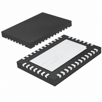
LTC3576EUFE#PBF Linear Technology, LTC3576EUFE#PBF Datasheet - Page 39

LTC3576EUFE#PBF
Manufacturer Part Number
LTC3576EUFE#PBF
Description
IC POWER MANAGER W/USB OTG 38QFN
Manufacturer
Linear Technology
Datasheet
1.LTC3576EUFEPBF.pdf
(48 pages)
Specifications of LTC3576EUFE#PBF
Applications
Handheld/Mobile Devices
Voltage - Supply
4.35 V ~ 5.5 V
Operating Temperature
-40°C ~ 85°C
Mounting Type
Surface Mount
Package / Case
38-QFN
Lead Free Status / RoHS Status
Lead free / RoHS Compliant
Current - Supply
-
Available stocks
Company
Part Number
Manufacturer
Quantity
Price
Hot Plugging and USB On-the-Go
If there is more than 4.3V on V
enabled, the bidirectional switching regulator will not try
to drive V
supply is then connected to V
happen depending on the properties of the external sup-
ply. If the external supply has a regulation voltage higher
than 5.1V, the bidirectional switching regulator will stop
switching and V
of the external supply. If the external supply has a lower
regulation voltage and is capable of only sourcing current
then V
will not source current to V
For a supply that can also sink current and has a regula-
tion voltage less than 5.1V, the bidirectional switching
regulator will source current into the external supply in an
attempt to bring V
supply holds V
bidirectional switching regulator will source up to 680mA
into the supply. If V
4V and V
off the switching regulator after 7.2ms. The CHRG pin will
then blink indicating a short circuit current fault.
V
Session Request Protocol
When two on-the-go devices are connected, one will be the
A device and the other will be the B device depending on
whether the device is connected to a micro A or micro B
plug. The A device provides power to the B device and
starts as the host. To prolong battery life, the A device can
power down V
device has powered down V
the A device to power up V
ing the session request protocol (SRP). The SRP consists
of data-line pulsing and V
fi rst pulse the D
pulse V
data-line pulse. The A device is required to respond to only
one of the pulsing methods. A devices that never power
down V
APPLICATIONS INFORMATION
BUS
Bypass Capacitance and USB On-The-Go
BUS
BUS
BUS
OUT
BUS
will be regulated to 5.1V. The external supply
are not required to respond to the SRP .
only if the A device does not respond to the
. If USB on-the-go is enabled and an external
+ 70mV then the short circuit timer will shut
BUS
BUS
+
BUS
or D
when the bus is not being used. If the A
BUS
BUS
to more than 4V or V
will be held at the regulation voltage
–
up to 5.1V. As long as the external
is held to a voltage that is less than
data line. The B device must then
BUS
BUS
BUS
BUS
BUS
pulsing. The B device must
and start a new session us-
.
, the B device can request
, one of three things will
BUS
when on-the-go is
OUT
+ 70mV, the
For V
the A device allows a B device to differentiate between
a powered down on-the-go device and a powered down
standard host. The B device will send out a pulse of current
that will raise V
connected to an on-the-go A device which must have no
more than 6.5μF . An on-the-go A device must drive V
as soon as the current pulse raises V
device is capable of responding to V
This same current pulse must not raise V
than 2V when connected to a standard host which must
have at least 96μF . The 96μF for a standard host represents
the minimum capacitance with V
5.25V. Since the SRP pulse must not drive V
than 2V, the capacitance seen at these voltage levels can be
greater than 96μF , especially if MLCCs are used. Therefore,
the 96μF represents a lower bound on the standard host
bypass capacitance for determining the amplitude and
duration of the current pulse. More capacitance will only
decrease the maximum level that V
given current pulse.
Figure 11 shows an on-the-go device using the LTC3576/
LTC3576-1 acting as the A device. Additional capacitance
can be placed on the V
when using the overvoltage protection circuit. A B device
may not be able to distinguish between a powered down
LTC3576/LTC3576-1 with overvoltage protection and a
powered down standard host because of this extra ca-
pacitance. In addition, if the SRP pulse raises V
its UVLO threshold of 4.3V the LTC3576/LTC3576-1 will
assume input power is available and will not attempt to
drive V
the-go device using the LTC3576/LTC3576-1 respond to
data-line pulsing.
When an on-the-go device using the LTC3576/LTC3576-1
becomes the B device, as in Figure 12, it must send out
a data line pulse followed by a V
session from the A device. The on-the-go device designer
can choose how much capacitance will be placed on the
V
a V
BUS
BUS
BUS
pin of the LTC3576/LTC3576-1 and then generate
BUS
pulse that can distinguish between a powered
pulsing, the limit on the V
. Therefore, it is recommended that an on-
BUS
LTC3576/LTC3576-1
to a voltage between 2.1V and 5.25V if
BUS
pin of the LTC3576/LTC3576-1
BUS
BUS
BUS
BUS
BUS
BUS
between 4.75V and
pulse to request a
above 2.1V if the
will rise to for a
pulsing.
capacitance on
BUS
BUS
any higher
BUS
39
greater
above
3576fb
BUS


