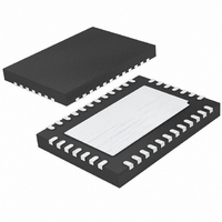
LTC3576EUFE#PBF Linear Technology, LTC3576EUFE#PBF Datasheet - Page 36

LTC3576EUFE#PBF
Manufacturer Part Number
LTC3576EUFE#PBF
Description
IC POWER MANAGER W/USB OTG 38QFN
Manufacturer
Linear Technology
Datasheet
1.LTC3576EUFEPBF.pdf
(48 pages)
Specifications of LTC3576EUFE#PBF
Applications
Handheld/Mobile Devices
Voltage - Supply
4.35 V ~ 5.5 V
Operating Temperature
-40°C ~ 85°C
Mounting Type
Surface Mount
Package / Case
38-QFN
Lead Free Status / RoHS Status
Lead free / RoHS Compliant
Current - Supply
-
Available stocks
Company
Part Number
Manufacturer
Quantity
Price
LTC3576/LTC3576-1
APPLICATIONS INFORMATION
It is possible to protect both V
overvoltage damage with several additional components,
as shown in Figure 7. Schottky diodes D1 and D2 pass the
larger of V1 and V2 to R1 and OVSENS. If either V1 or V2
exceeds 6V plus V
GND and both the WALL and USB inputs will be protected.
Each input is protected up to the drain-source breakdown,
BVDSS, of MN1 and MN2. R1 must also be rated for the
power dissipated during maximum overvoltage.
Reverse Voltage Protection
The LTC3576/LTC3576-1 can also be easily protected
against the application of reverse voltages, as shown in
Figure 8. D1 and R1 are necessary to limit the maximum
V
breakdown voltage must be safely below MP1’s BVGS. The
circuit shown in Figure 8 offers forward voltage protection
up to MN1’s BVDSS and reverse voltage protection up to
MP1’s BVDSS.
Battery Charger Over Programming
The USB high power specifi cation allows for up to 2.5W
to be drawn from the USB port. The LTC3576/LTC3576-1’s
bidirectional switching regulator in step-down mode
36
GS
seen by MP1 during positive overvoltage events. D1’s
V1
V2
Figure 7. Dual-Input Overvoltage Protection
D2
USB/WALL
ADAPTER
Figure 6. Overvoltage Protection
F
R1
(Schottky), OVGATE will be pulled to
R1
D1
MN1
M1
M2
C1
BUS
C1
V
OVGATE
OVSENS
LTC3576-1
LTC3576/
BUS
WALL
OVGATE
V
GND
OVSENS
BUS
LTC3576-1
LTC3576/
and WALL from
3576 F06
3576 F07
transforms the voltage at V
the level at BAT, while limiting power to less than the
amount programmed at CLPROG. The charger should be
programmed (with the PROG pin) to deliver the maximum
safe charging current without regard to the USB specifi -
cations. If there is insuffi cient current available to charge
the battery at the programmed rate, it will reduce charge
current until the system load on V
V
for more current than is available will not cause the aver-
age input current limit to be violated. It will merely allow
the battery charger to make use of all available power to
charge the battery as quickly as possible, and with minimal
dissipation within the charger.
Battery Charger Stability Considerations
The LTC3576/LTC3576-1’s battery charger contains both a
constant-voltage and a constant-current control loop. The
constant-voltage loop is stable without any compensation
when a battery is connected with low impedance leads.
Excessive lead length, however, may add enough series
inductance to require a bypass capacitor of at least 1μF
from BAT to GND.
High value, low ESR MLCCs reduce the constant-voltage
loop phase margin, possibly resulting in instability. Up
to 22μF may be used in parallel with a battery, but larger
capacitors should be decoupled with 0.2Ω to 1Ω of series
resistance.
Furthermore, a 100μF MLCC in series with a 0.3Ω resistor
from BAT to GND is required to prevent oscillation when
the battery is disconnected.
In constant-current mode, the PROG pin is in the feed-
back loop rather than the battery voltage. Because of the
additional pole created by any PROG pin capacitance,
BUS
USB/WALL
current limit is satisfi ed. Programming the charger
ADAPTER
V
V
BUS
BUS
Figure 8. Dual Polarity Voltage Protection
POSITIVE PROTECTION UP TO BVDSS OF MN1
NEGATIVE PROTECTION UP TO BVDSS OF MP1
MP1
R1
D1
R2
BUS
MN1
to a voltage just above
OUT
C1
is satisfi ed and the
V
OVGATE
OVSENS
LTC3576-1
LTC3576/
BUS
3576 F08
3576fb


