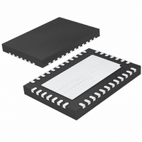
LTC3576EUFE#PBF Linear Technology, LTC3576EUFE#PBF Datasheet - Page 15

LTC3576EUFE#PBF
Manufacturer Part Number
LTC3576EUFE#PBF
Description
IC POWER MANAGER W/USB OTG 38QFN
Manufacturer
Linear Technology
Datasheet
1.LTC3576EUFEPBF.pdf
(48 pages)
Specifications of LTC3576EUFE#PBF
Applications
Handheld/Mobile Devices
Voltage - Supply
4.35 V ~ 5.5 V
Operating Temperature
-40°C ~ 85°C
Mounting Type
Surface Mount
Package / Case
38-QFN
Lead Free Status / RoHS Status
Lead free / RoHS Compliant
Current - Supply
-
Available stocks
Company
Part Number
Manufacturer
Quantity
Price
ACPR (Pin 28): External Power Source Present Output
(Active Low). ACPR indicates that the output of the external
high voltage step-down switching regulator is suitable for
use by the LTC3576/LTC3576-1. It should be connected to
the gate of an external P-channel MOSFET whose source
is connected to V
WALL. ACPR has a high level of V
GND. The USB bidirectional switcher is disabled when
ACPR is low.
PROG (Pin 29): Charge Current Program and Charge Cur-
rent Monitor Pin. Connecting a 1% resistor from PROG
to ground programs the charge current. If suffi cient input
power is available in constant-current mode, this pin servos
to 1V. The voltage on this pin always represents the actual
charge current by using the following formula:
CHRG (Pin 30): Open-Drain Charge Status Output. The
CHRG pin indicates the status of the battery charger.
Four possible charger states are represented by CHRG:
charging, not charging, unresponsive battery and battery
temperature out of range. In addition, CHRG is used to
indicate whether there is a short-circuit condition on V
when the bidirectional switching regulator is in step-up
mode (on-the-go). CHRG is modulated at 35kHz and
switches between a low and a high duty cycle for easy
recognition by either humans or microprocessors. See
Table 1. CHRG requires a pull-up resistor and/or LED to
provide indication.
IDGATE (Pin 31): Ideal Diode Amplifi er Output. This pin
controls the gate of an optional external P-channel MOSFET
used as an ideal diode between V
ideal diode operates in parallel with the internal ideal diode.
The source of the P-channel MOSFET should be connected
to V
external ideal diode MOSFET is not used, IDGATE should
be left fl oating.
PIN FUNCTIONS
I
BAT
OUT
=
and the drain should be connected to BAT. If the
R
V
PROG
PROG
• 1030
OUT
and whose drain is connected to
OUT
OUT
and BAT. The external
and a low level of
BUS
BAT (Pin 32): Single Cell Li-Ion Battery Pin. Depending on
available V
deliver power to V
from V
V
PowerPath Switching Regulator in step-down mode and
Input Voltage of the Battery Charger. The majority of the
portable product should be powered from V
LTC3576/LTC3576-1 will partition the available power
between the external load on V
tery charger. Priority is given to the external load and any
extra power is used to charge the battery. An ideal diode
from BAT to V
the load exceeds the allotted power from V
V
pin delivers power to V
be bypassed with a low impedance ceramic capacitor.
V
to V
a DC source such as a USB port or DC output wall adapter.
In on-the-go mode these pins provide power to external
loads. Tie the two V
with a low impedance multilayer ceramic capacitor.
SW (Pin 36): The SW pin transfers power between V
and V
the Applications Information section for a discussion of
inductance value and current rating.
I
limit of the PowerPath switching regulator. See Table 1.
Both the I
corresponding bits in the I
Each has a 2μA internal pull-down current source.
Exposed Pad (Pin 39): Ground. The Exposed Pad should
be connected to a continuous ground plane on the second
layer of the printed circuit board by several vias directly
under the LTC3576/LTC3576-1.
LIM0
OUT
BUS
BUS
OUT
, I
(Pins 34, 35): Power Pins. These pins deliver power
power source is removed. In on-the-go mode, this
OUT
(Pin 33): Output Voltage of the Bidirectional
LIM1
OUT
via the SW pin by drawing controlled current from
LIM0
via the bidirectional switching regulator. See
BUS
via the battery charger.
(Pins 37, 38): I
and I
OUT
power, a Li-Ion battery on BAT will either
LTC3576/LTC3576-1
OUT
BUS
ensures that V
LIM1
through the ideal diode or be charged
pins together at the part and bypass
BUS
pins are logically ORed with their
2
LIM0
C serial port. See Tables 3 and 6.
via the SW pin. V
and I
OUT
OUT
LIM1
and the internal bat-
is powered even if
control the current
BUS
OUT
OUT
or if the
15
should
. The
3576fb
BUS


