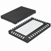
LTC3576EUFE#PBF Linear Technology, LTC3576EUFE#PBF Datasheet - Page 41

LTC3576EUFE#PBF
Manufacturer Part Number
LTC3576EUFE#PBF
Description
IC POWER MANAGER W/USB OTG 38QFN
Manufacturer
Linear Technology
Datasheet
1.LTC3576EUFEPBF.pdf
(48 pages)
Specifications of LTC3576EUFE#PBF
Applications
Handheld/Mobile Devices
Voltage - Supply
4.35 V ~ 5.5 V
Operating Temperature
-40°C ~ 85°C
Mounting Type
Surface Mount
Package / Case
38-QFN
Lead Free Status / RoHS Status
Lead free / RoHS Compliant
Current - Supply
-
Available stocks
Company
Part Number
Manufacturer
Quantity
Price
APPLICATIONS INFORMATION
the ideal diode of approximately 10mV. To minimize leakage,
the trace can be guarded on the PC board by surrounding
it with V
less than one volt higher than IDGATE.
When laying out the printed circuit board, the following
checklist should be used to ensure proper operation of
the LTC3576/LTC3576-1:
1. The Exposed Pad of the package (Pin 39) should
2. The traces connecting V
3. Connections between the step-down switching regu-
connect directly to a large ground plane to minimize
thermal and electrical impedance.
V
to their respective decoupling capacitors should be
as short as possible. The GND side of these capaci-
tors should connect directly to the ground plane of
the part. These capacitors provide the AC current to
the internal power MOSFETs and their drivers. It is
critical to minimize inductance from these capacitors
to the LTC3576/LTC3576-1 and external step-down
switching regulator.
lator (both internal and external) inductors and their
respective output capacitors should be kept as short
IN
of the external step-down switching regulator
OUT
connected metal, which should generally be
BUS
, V
Figure 13. Higher Frequency Ground Current Follow Their
Incident Path. Slices in the Ground Plane Create Large Loop
Areas. The Large Loop Areas Increase the Inductance of the
Path Leading to Higher System Noise
IN1
, V
IN2
, V
IN3
and
4. The switching power traces connecting SW, SW1,
5. Keep the feedback pin traces (FB1, FB2, FB3 and FB
6. Connect V
as possible. Use area fi lls whenever possible. This
also applies to the PowerPath switching regulator
inductor and the output capacitor on V
side of the output capacitors should connect directly
to the thermal ground plane of the part.
SW2, SW3 and the switch node of the external step-
down switching regulator to their respective induc-
tors should be minimized to reduce radiated EMI and
parasitic coupling. Due to the large voltage swing
of the switching nodes, sensitive nodes such as the
feedback nodes (FB1, FB2 and FB3) should be kept
far away or shielded from the switching nodes or
poor performance could result.
of the external step-down switching regulator) as
short as possible. Minimize any parasitic capacitance
between the feedback traces and any switching node
(i.e., SW, SW1, SW2, SW3 and logic signals). If nec-
essary shield the feedback nodes with a GND trace
low impedance trace.
3576 F13
IN1
, V
LTC3576/LTC3576-1
IN2
and V
IN3
to V
OUT
through a short
OUT
. The GND
41
3576fb


