TB6582FG(O,EL) Toshiba, TB6582FG(O,EL) Datasheet - Page 8
TB6582FG(O,EL)
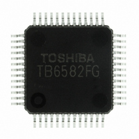
Manufacturer Part Number
TB6582FG(O,EL)
Description
IC BRUSHLESS MOTOR CTLR 52-QFP
Manufacturer
Toshiba
Type
3 Phase Full Wave Brushless Motor Controllerr
Datasheet
1.TB6582FGOEL.pdf
(28 pages)
Specifications of TB6582FG(O,EL)
Applications
DC Motor Controller, Brushless (BLDC), 3 Phase
Number Of Outputs
1
Voltage - Supply
6.5 V ~ 16.5 V
Operating Temperature
-30°C ~ 115°C
Mounting Type
Surface Mount
Package / Case
52-QFP
Product
Fan / Motor Controllers / Drivers
Operating Supply Voltage
15 V
Supply Current
16 mA
Mounting Style
SMD/SMT
Lead Free Status / RoHS Status
Lead free / RoHS Compliant
Current - Output
-
Voltage - Load
-
Lead Free Status / Rohs Status
Lead free / RoHS Compliant
Other names
TB6582FG(O,EL)
TB6582FGOELTR
TB6582FGOELTR
Available stocks
Company
Part Number
Manufacturer
Quantity
Price


Electrical Characteristics
Power supply current
Input current
Input voltage
Output duty cycle
(max)
Input delay
Charge current for SC
Threshold voltage for
mode switching from
DC excitation mode to
forced commutation
mode
Output voltage
Output leakage
current
Output off time by
high/low-side
transistor
PWM frequency
(Carrier frequency)
Reverse rotation
brake
Motor power supply
monitor
V
CC
Characteristics
monitor
V
V
V
V
in (1)
in (2)
in (3)
V
V
Ton (max)
V
V
V
sp
V
V
OUT (H)-1
V
Symbol
OUT (L)-1
V
V
COM
V
COM
V
REV (H)
V
V
REV (L)
V
I
I
I
I
I
I
T
I
CC
FG (H)
I
CC
T
FG (L)
in (1)
in (2)
in (3)
in (4)
in (5)
in (6)
I
refout
L (H)
I
V
L (L)
H (1)
H (2)
H (3)
OFF
F
BRK
CC
SC
DC
IP
C
(H)
(L)
(H)
(L)
M
H
H
H
H
L
L
L
L
(Ta = 25°C, V
V
V
V
V
V
V
V
EP, CW/CCW, FGC, FRCDRV
FST, FGC, FRCDRV
Sys.RES
Modulation wave: 90% typ.
Start motor operation
OSC/C = 390 pF, OSC/R = 6.8 kΩ
V
Icut when in sine-wave mode OSC = 5 MHz
DC excitation mode
DC excitation → forced commutation
Hysteresis
I
I
I
I
I
I
I
V
V
OSC = 5 MHz, I
OSC/C = 390 pF, OSC/R = 6.8 kΩ
V
reverse rotation start
Drive output off
Drive output restart
Input hysteresis width
Output start point
Output stop point
Input hysteresis width
Design Specifications
OUT
OUT
OUT
OUT
OUT
OUT
OUT
refout
in
in
in
in
in
in
sp
OUT
OUT
BRK
= 0 V
= 5 V
= 0 V
= 5 V
= 0 V
= 5 V
= 5.7 V
= 2 mA
= −2 mA
= 1 mA
= −1 mA
= 1 mA
= −1 mA
= 5 mA
=
= 0 V
= 5 V
= OPEN
1.5
V, OSC = 5 MHz,
V
FRCDRV
Sys.RES
Sys.RES
V
EP, CW/CCW, FGC, FRCDRV, Fst
sp
sp
, V
OUT
, EP, CW/CCW, FGC, V
CC
Test condition
LA
= ± 2 mA
= 15 V)
UH, UL, VH, VL, WH, WL
UH, UL, VH, VL, WH, WL
REV
REV
FG
FG
V
UH, UL, VH, VL, WH, WL
UH, UL, VH, VL, WH, WL
refout
8
LA
V
V
V
V
V
−100
− 0.5
− 1.0
− 1.0
1.75
−10
Min
refout
refout
refout
refout
refout
− 1
4.0
2.0
− 1
5.1
1.8
0.6
0.3
4.5
1.5
2.1
4.2
3.7
−6
87
18
5
0
Preliminary
V
V
V
− 0.2
− 0.2
− 0.2
(2.0)
Typ.
1.85
0.35
−50
±12
refout
refout
refout
5.4
2.1
1.2
0.5
0.2
0.2
0.2
5.0
1.8
2.2
4.5
4.0
0.5
10
25
50
−3
90
20
52
0
0
0
0
V
V
V
Max
1.95
100
refout
refout
refout
0.8
3.0
1.0
0.7
5.7
2.4
1.8
0.7
0.5
1.0
1.0
5.5
2.1
2.3
4.8
4.3
50
93
16
10
22
TB6582FG
2007-10-18
Unit
kHz
mA
mV
µA
µA
µA
µs
µs
%
%
V
V
V
V
V
V
V
V
Related parts for TB6582FG(O,EL)
Image
Part Number
Description
Manufacturer
Datasheet
Request
R

Part Number:
Description:
IC BRUSHLESS MOTOR CTLR 52-QFP
Manufacturer:
Toshiba
Datasheet:

Part Number:
Description:
Toshiba Semiconductor [TOSHIBA IGBT Module Silicon N Channel IGBT]
Manufacturer:
TOSHIBA Semiconductor CORPORATION
Datasheet:
Part Number:
Description:
TOSHIBA GTR MODULE SILICON NPN TRIPLE DIFFUSED TYPE
Manufacturer:
TOSHIBA Semiconductor CORPORATION
Datasheet:
Part Number:
Description:
TOSHIBA GTR Module Silicon N Channel IGBT
Manufacturer:
TOSHIBA Semiconductor CORPORATION
Datasheet:
Part Number:
Description:
TOSHIBA Intelligent Power Module Silicon N Channel IGBT
Manufacturer:
TOSHIBA Semiconductor CORPORATION
Datasheet:
Part Number:
Description:
TOSHIBA INTELLIGENT POWER MODULE SILICON N CHANNEL LGBT
Manufacturer:
TOSHIBA Semiconductor CORPORATION
Datasheet:
Part Number:
Description:
TOSHIBA IGBT Module Silicon N Channel IGBT
Manufacturer:
TOSHIBA Semiconductor CORPORATION
Datasheet:
Part Number:
Description:
TOSHIBA GTR MODULE SILICON N−CHANNEL IGBT
Manufacturer:
TOSHIBA Semiconductor CORPORATION
Datasheet:
Part Number:
Description:
TOSHIBA Intelligent Power Module Silicon N Channel IGBT
Manufacturer:
TOSHIBA Semiconductor CORPORATION
Datasheet:
Part Number:
Description:
TOSHIBA GTR Module Silicon N Channel IGBT
Manufacturer:
TOSHIBA Semiconductor CORPORATION
Datasheet:
Part Number:
Description:
TOSHIBA INTELLIGENT POWER MODULE
Manufacturer:
TOSHIBA Semiconductor CORPORATION
Datasheet:
Part Number:
Description:
TOSHIBA Intelligent Power Module Silicon N Channel IGBT
Manufacturer:
TOSHIBA Semiconductor CORPORATION
Datasheet:
Part Number:
Description:
TOSHIBA Intelligent Power Module Silicon N Channel IGBT
Manufacturer:
TOSHIBA Semiconductor CORPORATION
Datasheet:
Part Number:
Description:
TOSHIBA IGBT Module Silicon N Channel IGBT
Manufacturer:
TOSHIBA Semiconductor CORPORATION
Datasheet:
Part Number:
Description:
TOSHIBA Intelligent Power Module Silicon N Channel IGBT
Manufacturer:
TOSHIBA Semiconductor CORPORATION
Datasheet: