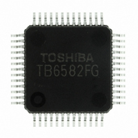
TB6582FG(O,EL) Toshiba, TB6582FG(O,EL) Datasheet - Page 16

TB6582FG(O,EL)
Manufacturer Part Number
TB6582FG(O,EL)
Description
IC BRUSHLESS MOTOR CTLR 52-QFP
Manufacturer
Toshiba
Type
3 Phase Full Wave Brushless Motor Controllerr
Datasheet
1.TB6582FGOEL.pdf
(28 pages)
Specifications of TB6582FG(O,EL)
Applications
DC Motor Controller, Brushless (BLDC), 3 Phase
Number Of Outputs
1
Voltage - Supply
6.5 V ~ 16.5 V
Operating Temperature
-30°C ~ 115°C
Mounting Type
Surface Mount
Package / Case
52-QFP
Product
Fan / Motor Controllers / Drivers
Operating Supply Voltage
15 V
Supply Current
16 mA
Mounting Style
SMD/SMT
Lead Free Status / RoHS Status
Lead free / RoHS Compliant
Current - Output
-
Voltage - Load
-
Lead Free Status / Rohs Status
Lead free / RoHS Compliant
Other names
TB6582FG(O,EL)
TB6582FGOELTR
TB6582FGOELTR
Available stocks
Company
Part Number
Manufacturer
Quantity
Price
Note 1: Determining the capacitor value of C
Note 2: Since drive signals are generated by the calculated induced voltage, the outputs of those signals are
Resolution
< Determination Procedure >
< Target Operation >
(1)
(2)
(3)
(4)
The external capacitor C
voltage calculation. A capacitor of the same value as C
checking the basic operations. Since the appropriate capacitance and resistance of the external
components vary depending on the motor type, they must be adjusted experimentally.
When FGC = 2.5 V, the internally-detected induced voltage is generated from the REV pin as a
square-wave signal. This signal is delayed by the amount of time specified by C
1
2
3
4
5
6
7
8
U-phase output
REV (22 pin)
The difference between the zero-cross point of the induced voltage generated at the U-phase output
and the one of the induced voltage calculated by the TB6582FG should be measured by experiment
while the motor is operating in square-wave drive (120° commutation) mode. The C
should be specified corresponding to the measurement result.
When the motor is driven by the square wave (120° commutation), an input voltage of 2.5 V must
be applied to the FGC pin. When FGC = 2.5 V, the TB6582FG enters into Test mode and the REV
pin generates an induced voltage output of phase U calculated internally.
The motor should be operated with a rotation speed appropriate for the normal usage (, such as
700 rpm) in 120° commutation by applying an appropriate voltage to the V
Measure the difference (∆Y
output.
The capacitor value of C
enabled with a certain delay time. Though the automatic lead-angle correction is applied, the lead
angle can also be adjusted in the early stages. The range of the lead-angle correction is from 0° to
112.5° and the four-bit resolution (16 steps) can be programmed.
Analog input to the VLA pin (0 to 5 V range is resolved to 16 steps)
0 V = 0°
5.0 V = 112.5°
0.312 to 0.625
0.625 to 0.937
1.250 to 1.562
1.562 to 1.875
1.875 to 2.187
2.187 to 2.500
Table 1. C
0.937 to 1.25
0 to 0.312
VLA (V)
240 V
GND
GND
5 V
2
LA
Design Specifications
considerably affects the factor that causes the delay time in the induced
60°
Lead angle value (°)
Values Corresponding to the Delay Time ∆Y
LA
should be determined according to the delay time (∆Y
T
120°
∆Y
) between the zero-cross points of the U-phase output and the REV
30°
60°
22.5
37.5
52.5
7.5
15
30
45
0
T
30°
LA
Figure 1
∆Y
16
T
Resolution
10
11
12
13
14
15
16
9
2
(103)
(223)
(473)
C
should be connected to the C
LA
2.812 to 3.125
3.125 to 3.437
3.437 to 3.750
3.750 to 4.062
4.062 to 4.375
4.375 to 4.687
2.50 to 2.812
4.687 to 5.0
VLA (V)
Preliminary
Lead angle value (°)
T
LA
(Hys. = 0.1 V)
SP
.
pin.
LA
112.5
97.5
67.5
82.5
105
60
75
90
T
LA
).
pin while
TB6582FG
capacitor value
2007-10-18


