LP3950SL/NOPB National Semiconductor, LP3950SL/NOPB Datasheet - Page 25
LP3950SL/NOPB
Manufacturer Part Number
LP3950SL/NOPB
Description
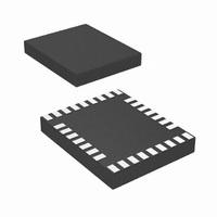
IC LED DRVR WHITE BCKLGT 32-TSCP
Manufacturer
National Semiconductor
Series
PowerWise®r
Type
Backlight, White LED (I²C Interface)r
Datasheet
1.LP3950SLNOPB.pdf
(31 pages)
Specifications of LP3950SL/NOPB
Topology
PWM, Step-Up (Boost)
Number Of Outputs
6
Internal Driver
Yes
Type - Primary
Flash/Torch, LED Blinker, Light Management Unit (LMU)
Type - Secondary
RGB, White LED
Frequency
2MHz
Voltage - Supply
2.7 V ~ 2.9 V
Voltage - Output
5V
Mounting Type
Surface Mount
Package / Case
32-Laminate TCSP
Operating Temperature
-40°C ~ 85°C
Internal Switch(s)
Yes
Efficiency
90%
Led Driver Application
Mobile Phone Display Lighting, General LED Lighting
No. Of Outputs
6
Output Current
300mA
Output Voltage
5.3V
Input Voltage
3V To 7.2V
Rohs Compliant
Yes
Lead Free Status / RoHS Status
Lead free / RoHS Compliant
Current - Output / Channel
-
Other names
LP3950SL/CSP1
LP3950SLTR
LP3950SLTR


Symbol
C
C
C
C
C
C
C
R
R
C
L
D
R
Recommended External
Components
OUTPUT CAPACITOR, C
The output capacitor C
the output ripple voltage. In general, the higher the value of
C
ramic capacitors with low ESR (Equivalent Series Resis-
tance) are the best choice. At the lighter loads, the low ESR
ceramics offer a much lower V
ESR tantalums of the same value. At the higher loads, the
ceramics offer a slightly lower V
the tantalums of the same value. However, the dv/dt of the
V
ums under all load conditions. Capacitor voltage rating must
be sufficient, 10V is recommended.
Some ceramic capacitors, especially those in small
packages, exhibit a strong capacitance reduction with
the increased applied voltage. The capacitance value
can fall to below half of the nominal capacitance. Too
low output capacitance can make the boost converter
unstable.
INPUT CAPACITOR, C
The input capacitor C
input ripple voltage and to a lesser degree the V
higher value C
age rating must be sufficient, 10V is recommended.
OUTPUT DIODE, D
A Schottky diode should be used for the output diode. To
maintain high efficiency the average current rating of the
schottky diode should be larger than the peak inductor cur-
1
Note 19: Resistor RT tolerance change will change the timing accuracy of RGB block. Also the boost converter switching frequency will be affected.
PCB Design Guidelines
Printed circuit board layout is critical to low noise operation
and good performance of the LP3950. Bypass capacitors
should be close to the V
Special attention must be given to the routing of the switch-
ing loops. Lengths of these loops should be minimized. It is
essential to place the input capacitor, the output capacitor,
VDD1
VDD2
OUT
IN
VDDIO
VDDA
1,2,3
T
SO
VREF
1
RX
OUT
OUT
, R
, the lower the output ripple magnitude. Multilayer ce-
GX
ripple with the ceramics is much lower that the tantal-
, R
BX
IN
V
V
Output Capacitor from FB to GND
Input Capacitor from Battery Voltage to GND
V
V
Audio Input Capacitors
Oscillator Frequency Bias Resistor
SO Output Pull-up Resistor
Reference Voltage Capacitor, between V
Boost Converter Inductor
Rectifying Diode, V
RGB LED
Red, Green, Blue or White LEDs
Current Limit Resistors
will give a lower V
DD1
DD2
DD_IO
DDA
1
IN
Bypass Capacitor
Bypass Capacitor
Bypass Capacitor
OUT
IN
directly affects the magnitude of the
Bypass Capacitor
OUT
DD
directly affects the magnitude of
pins of the integrated circuit.
OUT
OUT
Symbol Explanation
IN
F
ripple than the higher
ripple magnitude than
ripple. Capacitor volt-
@
List of Recommended External Components
Maxload
OUT
ripple. A
REF
and GND
25
rent (
fast switching speeds are ideal for increasing efficiency in
portable applications. Choose a reverse breakdown of the
schottky diode larger than the output voltage. Do not use
ordinary rectifier diodes, since slow switching speeds and
long recovery times cause the efficiency and the load regu-
lation to suffer.
INDUCTOR, L
LP3950’s high switching frequency enables the use of a
small surface mount inductor. A 4.7 µH shielded inductor is
suggested for 2.0 MHz switching frequency. Values below
2.2 µH should not be used at 2.0 MHz. At lower switching
frequencies 4.7 µH inductors should always be used. The
inductor should have a saturation current rating higher than
the peak current it will experience during circuit operation
(
efficiency. Open core inductors cause flux linkage with circuit
components and, thus, may interfere with the normal opera-
tion of the circuit. This should be avoided. For high efficiency,
choose an inductor with a high frequency core material such
as ferrite to reduce the core losses. To minimize radiated
noise, use a toroid, pot core or shielded core inductor. The
inductor should be connected to the SW pin as close to the
IC as possible. Examples of suitable inductors are TDK type
VLF4012AT- 4R7M1R1 and Coilcraft type MSS4020-
472MLD.
the inductor and the schottky diode very close to the inte-
grated circuit and use wide routings for those components.
Sensitive components should be placed far from those com-
ponents with high pulsating current. A ground plane is rec-
ommended.
The power switch loop (the switch is on) has the greatest
affect on noise generation. The loop is formed by the input
A
1.0A). Less than 300 mΩ ESR is suggested for high
A
1.0A). Schottky diodes with a low forward drop and
10
10
Value
100
100
100
±
±
100
100
100
4.7
0.3
10
82
10%
10%
1
Unit
kΩ
kΩ
µH
nF
nF
µF
µF
nF
nF
nF
nF
V
User Defined
Ceramic, X5R
Ceramic, X5R
Ceramic, X5R
Ceramic, X5R
Ceramic, X5R
Ceramic, X5R
Ceramic, X5R
1% (Note 19)
Ceramic, X5R
Shielded, Low ESR, I
Schottky Diode
Type
www.national.com
SAT
A
1.0A
Related parts for LP3950SL/NOPB
Image
Part Number
Description
Manufacturer
Datasheet
Request
R

Part Number:
Description:
Color LED Driver with Audio Synchronizer
Manufacturer:
NSC [National Semiconductor]
Datasheet:

Part Number:
Description:
National Semiconductor [8-Bit D/A Converter]
Manufacturer:
National Semiconductor
Datasheet:
Part Number:
Description:
National Semiconductor [Media Coprocessor]
Manufacturer:
National Semiconductor
Datasheet:
Part Number:
Description:
Digitally Controlled Tone and Volume Circuit with Stereo Audio Power Amplifier, Microphone Preamp Stage and National 3D Sound
Manufacturer:
National Semiconductor
Datasheet:
Part Number:
Description:
Digitally Controlled Tone and Volume Circuit with Stereo Audio Power Amplifier, Microphone Preamp Stage and National 3D Sound
Manufacturer:
National Semiconductor
Datasheet:
Part Number:
Description:
AC97 Rev 2 Codec with Sample Rate Conversion and National 3D Sound
Manufacturer:
National Semiconductor
Part Number:
Description:
Manufacturer:
National Semiconductor
Datasheet:
Part Number:
Description:
Manufacturer:
National Semiconductor
Datasheet:
Part Number:
Description:
General Purpose, Low Voltage, Low Power, Rail-to-Rail Output Operational Amplifiers
Manufacturer:
National Semiconductor
Datasheet:
Part Number:
Description:
8-bit 20 MSPS flash A/D converter.
Manufacturer:
National Semiconductor
Datasheet:
Part Number:
Description:
Low Noise Quad Operational Amplifier
Manufacturer:
National Semiconductor
Datasheet:
Part Number:
Description:
Quad Differential Line Receivers
Manufacturer:
National Semiconductor
Datasheet:
Part Number:
Description:
Quad High Speed Trapezoidal? Bus Transceiver
Manufacturer:
National Semiconductor
Datasheet:
Part Number:
Description:
Dual Line Receiver
Manufacturer:
National Semiconductor
Datasheet: