LP3950SL/NOPB National Semiconductor, LP3950SL/NOPB Datasheet - Page 20
LP3950SL/NOPB
Manufacturer Part Number
LP3950SL/NOPB
Description
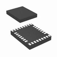
IC LED DRVR WHITE BCKLGT 32-TSCP
Manufacturer
National Semiconductor
Series
PowerWise®r
Type
Backlight, White LED (I²C Interface)r
Datasheet
1.LP3950SLNOPB.pdf
(31 pages)
Specifications of LP3950SL/NOPB
Topology
PWM, Step-Up (Boost)
Number Of Outputs
6
Internal Driver
Yes
Type - Primary
Flash/Torch, LED Blinker, Light Management Unit (LMU)
Type - Secondary
RGB, White LED
Frequency
2MHz
Voltage - Supply
2.7 V ~ 2.9 V
Voltage - Output
5V
Mounting Type
Surface Mount
Package / Case
32-Laminate TCSP
Operating Temperature
-40°C ~ 85°C
Internal Switch(s)
Yes
Efficiency
90%
Led Driver Application
Mobile Phone Display Lighting, General LED Lighting
No. Of Outputs
6
Output Current
300mA
Output Voltage
5.3V
Input Voltage
3V To 7.2V
Rohs Compliant
Yes
Lead Free Status / RoHS Status
Lead free / RoHS Compliant
Current - Output / Channel
-
Other names
LP3950SL/CSP1
LP3950SLTR
LP3950SLTR


www.national.com
Audio Synchronization
INPUT BUFFERING
Figure 16 describes the LP3950 audio input buffering struc-
ture in high level. The electric parameters of the buffers are
described in Table Audio Synchronization Characteristics.
Operational amplifiers for both buffers are rail-to-rail input
opamps. The single ended buffer is simply a voltage follower.
DC level of the input signal is generated by a resistor divider.
The differential amplifier is a basic differential-to-single-
ended converter.
Schematic Diagram
Functional Block Diagram
The digitized input signal has a DC component that is re-
moved by the digital DC REMOVER (-3 dB
automatic GAIN CONTROL adjusts the input signal to suit-
able range automatically. User can disable AGC and the gain
can be set manually with PROGRAMMABLE GAIN. The
LP3950 has two audio synchronization modes: amplitude
and frequency. For amplitude based synchronization the
PEAK DETECTION method is used. For frequency based
FIGURE 16. Audio Input Buffer Structure
(Continued)
FIGURE 17. Signal Path Block Diagram
@
A
400 Hz). The
20129331
20
AUDIO SYNCHRONIZATION SIGNAL PATH
LP3950 audio synchronization is mainly done digitally and it
consists of following signal path blocks (see Figure 17)
• Input buffers
• Multiplexer
• AD converter
• DC remover
• Automatic gain control (AGC) / programmable gain
• 3 band digital filter
• Peak detector
• Look-up tables (LUT)
• Mode selector
• Integrators
• PWM generator
synchronization the three-way crossover FILTER separates
high pass, low pass and band pass signals. For both modes,
a predefined lookup table (LUT) is used to match the audio
visual effect. The MODE SELECTOR selects the synchroni-
zation mode. Reaction speed can be selected using INTE-
GRATOR speed variables. Finally PWM GENERATOR sets
the driver FETs duty cycles.
20129332
Related parts for LP3950SL/NOPB
Image
Part Number
Description
Manufacturer
Datasheet
Request
R

Part Number:
Description:
Color LED Driver with Audio Synchronizer
Manufacturer:
NSC [National Semiconductor]
Datasheet:

Part Number:
Description:
National Semiconductor [8-Bit D/A Converter]
Manufacturer:
National Semiconductor
Datasheet:
Part Number:
Description:
National Semiconductor [Media Coprocessor]
Manufacturer:
National Semiconductor
Datasheet:
Part Number:
Description:
Digitally Controlled Tone and Volume Circuit with Stereo Audio Power Amplifier, Microphone Preamp Stage and National 3D Sound
Manufacturer:
National Semiconductor
Datasheet:
Part Number:
Description:
Digitally Controlled Tone and Volume Circuit with Stereo Audio Power Amplifier, Microphone Preamp Stage and National 3D Sound
Manufacturer:
National Semiconductor
Datasheet:
Part Number:
Description:
AC97 Rev 2 Codec with Sample Rate Conversion and National 3D Sound
Manufacturer:
National Semiconductor
Part Number:
Description:
Manufacturer:
National Semiconductor
Datasheet:
Part Number:
Description:
Manufacturer:
National Semiconductor
Datasheet:
Part Number:
Description:
General Purpose, Low Voltage, Low Power, Rail-to-Rail Output Operational Amplifiers
Manufacturer:
National Semiconductor
Datasheet:
Part Number:
Description:
8-bit 20 MSPS flash A/D converter.
Manufacturer:
National Semiconductor
Datasheet:
Part Number:
Description:
Low Noise Quad Operational Amplifier
Manufacturer:
National Semiconductor
Datasheet:
Part Number:
Description:
Quad Differential Line Receivers
Manufacturer:
National Semiconductor
Datasheet:
Part Number:
Description:
Quad High Speed Trapezoidal? Bus Transceiver
Manufacturer:
National Semiconductor
Datasheet:
Part Number:
Description:
Dual Line Receiver
Manufacturer:
National Semiconductor
Datasheet: