LP3950SL/NOPB National Semiconductor, LP3950SL/NOPB Datasheet - Page 10
LP3950SL/NOPB
Manufacturer Part Number
LP3950SL/NOPB
Description
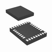
IC LED DRVR WHITE BCKLGT 32-TSCP
Manufacturer
National Semiconductor
Series
PowerWise®r
Type
Backlight, White LED (I²C Interface)r
Datasheet
1.LP3950SLNOPB.pdf
(31 pages)
Specifications of LP3950SL/NOPB
Topology
PWM, Step-Up (Boost)
Number Of Outputs
6
Internal Driver
Yes
Type - Primary
Flash/Torch, LED Blinker, Light Management Unit (LMU)
Type - Secondary
RGB, White LED
Frequency
2MHz
Voltage - Supply
2.7 V ~ 2.9 V
Voltage - Output
5V
Mounting Type
Surface Mount
Package / Case
32-Laminate TCSP
Operating Temperature
-40°C ~ 85°C
Internal Switch(s)
Yes
Efficiency
90%
Led Driver Application
Mobile Phone Display Lighting, General LED Lighting
No. Of Outputs
6
Output Current
300mA
Output Voltage
5.3V
Input Voltage
3V To 7.2V
Rohs Compliant
Yes
Lead Free Status / RoHS Status
Lead free / RoHS Compliant
Current - Output / Channel
-
Other names
LP3950SL/CSP1
LP3950SLTR
LP3950SLTR


www.national.com
I
I
In I
I
these signals need a pull-up resistor according to I
fication. The values of the pull-up resistors are determined
by the capacitance of the bus (typ.
specifications are shown in Table I
Unused pin SO can be left unconnected and pin SI must be
I
START and STOP bits classify the beginning and the end of
the I
transition from HIGH to LOW while SCL line is HIGH. STOP
condition is defined as the SDA transition from LOW to HIGH
while SCL is HIGH. The I
2
2
2
2
C SIGNALS
C clock and the SDA pin is used for the I
C START AND STOP CONDITIONS
C Compatible Interface
2
C compatible mode, the LP3950 pin SCL is used for the
2
C session. START condition is defined as SDA signal
Note: Data guaranteed by design.
V
DD1
Symbol
10
12
11
1
2
3
4
5
6
7
8
9
= V
DD2
Cycle Time
Enable Lead Time
Enable Lag Time
Clock Low Time
Clock High Time
Data Setup Time
Data Hold Time
Data Access Time
Output Disable Time
Output Data Valid
Output Data Hold Time
SS Inactive Time
= V
2
C master always generates
DDA
2
= 2.70V to 2.90V, V
C Timing Parameters .
A
1.8k). Signal timing
FIGURE 5. I
Parameter
2
C data. Both
2
SPI Timing Parameters
C speci-
DDIO
2
C Signals: Data Validity
= 1.80V to V
10
connected to V
rate is 400 kbit/s (V
interface can be used down to 1.65 V
rate of 200 kbit/s.
I
The data on the SDA line must be stable during the HIGH
period of the clock signal (SCL). In other words, state of the
data line can only be changed when CLK is LOW.
START and STOP bits. The I
after START condition and free after STOP condition. During
data transmission, the I
START conditions. First START and repeated START condi-
tions are equivalent, function-wise.
2
C DATA VALIDITY
DD1,2
Min
V
80
40
40
40
40
20
15
0
0
DDIO
20129310
Limit
or GND (address selector). Maximum bit
DDIO
Max
2
1.80V to V
27
27
37
C master can generate repeated
2
C bus is considered to be busy
DD1,2
Units
DDIO
ns
ns
ns
ns
ns
ns
ns
ns
ns
ns
ns
ns
V). I
with maximum bit
2
C compatible
Related parts for LP3950SL/NOPB
Image
Part Number
Description
Manufacturer
Datasheet
Request
R

Part Number:
Description:
Color LED Driver with Audio Synchronizer
Manufacturer:
NSC [National Semiconductor]
Datasheet:

Part Number:
Description:
National Semiconductor [8-Bit D/A Converter]
Manufacturer:
National Semiconductor
Datasheet:
Part Number:
Description:
National Semiconductor [Media Coprocessor]
Manufacturer:
National Semiconductor
Datasheet:
Part Number:
Description:
Digitally Controlled Tone and Volume Circuit with Stereo Audio Power Amplifier, Microphone Preamp Stage and National 3D Sound
Manufacturer:
National Semiconductor
Datasheet:
Part Number:
Description:
Digitally Controlled Tone and Volume Circuit with Stereo Audio Power Amplifier, Microphone Preamp Stage and National 3D Sound
Manufacturer:
National Semiconductor
Datasheet:
Part Number:
Description:
AC97 Rev 2 Codec with Sample Rate Conversion and National 3D Sound
Manufacturer:
National Semiconductor
Part Number:
Description:
Manufacturer:
National Semiconductor
Datasheet:
Part Number:
Description:
Manufacturer:
National Semiconductor
Datasheet:
Part Number:
Description:
General Purpose, Low Voltage, Low Power, Rail-to-Rail Output Operational Amplifiers
Manufacturer:
National Semiconductor
Datasheet:
Part Number:
Description:
8-bit 20 MSPS flash A/D converter.
Manufacturer:
National Semiconductor
Datasheet:
Part Number:
Description:
Low Noise Quad Operational Amplifier
Manufacturer:
National Semiconductor
Datasheet:
Part Number:
Description:
Quad Differential Line Receivers
Manufacturer:
National Semiconductor
Datasheet:
Part Number:
Description:
Quad High Speed Trapezoidal? Bus Transceiver
Manufacturer:
National Semiconductor
Datasheet:
Part Number:
Description:
Dual Line Receiver
Manufacturer:
National Semiconductor
Datasheet: