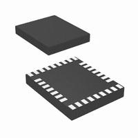
LP3950SL/NOPB National Semiconductor, LP3950SL/NOPB Datasheet - Page 17

LP3950SL/NOPB
Manufacturer Part Number
LP3950SL/NOPB
Description
IC LED DRVR WHITE BCKLGT 32-TSCP
Manufacturer
National Semiconductor
Series
PowerWise®r
Type
Backlight, White LED (I²C Interface)r
Datasheet
1.LP3950SLNOPB.pdf
(31 pages)
Specifications of LP3950SL/NOPB
Topology
PWM, Step-Up (Boost)
Number Of Outputs
6
Internal Driver
Yes
Type - Primary
Flash/Torch, LED Blinker, Light Management Unit (LMU)
Type - Secondary
RGB, White LED
Frequency
2MHz
Voltage - Supply
2.7 V ~ 2.9 V
Voltage - Output
5V
Mounting Type
Surface Mount
Package / Case
32-Laminate TCSP
Operating Temperature
-40°C ~ 85°C
Internal Switch(s)
Yes
Efficiency
90%
Led Driver Application
Mobile Phone Display Lighting, General LED Lighting
No. Of Outputs
6
Output Current
300mA
Output Voltage
5.3V
Input Voltage
3V To 7.2V
Rohs Compliant
Yes
Lead Free Status / RoHS Status
Lead free / RoHS Compliant
Current - Output / Channel
-
Other names
LP3950SL/CSP1
LP3950SLTR
LP3950SLTR
R
I
t
t
t
t
Duty
t
D
D
D
D
f
f
LEAKAGE
SMAX
SMIN
SRES
START/STOP
BLINK
PWMF
PWM
RDUTY[3:0]
GDUTY[3:0]
BDUTY[3:0]
RSLOPE[3:0]
GSLOPE[3:0]
BSLOPE[3:0]
RON[3:0]
GON[3:0]
BON[3:0]
DS-ON
CYCF
CYC
RESF
RES
Programmable Pattern Mode
RGB Driver Characteristics
(R1, G1, B1, R2, G2, B2 outputs). Limits in standard typeface are for T
ating ambient temperature range (−40˚C ≤ T
RGB LED PWM Control
(Continued)
Symbol
FIGURE 14. Example Blinking Waveforms
ON Resistance
Off State Leakage Current
Maximum Slope Period
Minimum Slope Period
Slope Resolution
Start/Stop Resolution
Duty Step Size
Blinking Cycle Accuracy
Duty Cycle Range
Duty Cycle Range
Duty Resolution
Duty Resolution
PWM Frequency
PWM Frequency
DUTY sets the brightness of the LED by adjusting the duty cycle of the PWM driver. The minimum DUTY
cycle is 0% [0000] and the maximum in the flash mode is
determined by the external resistor, LED forward voltage drop and the boost voltage. In the normal mode
the maximum duty cycle is 33%.
SLOPE sets the turn-on and turn-off slopes. Fastest slope is set by [0000] and slowest by [1111]. SLOPE
changes the duty cycle at constant, programmable rate. For each slope setting the maximum slope time
appears at maximum DUTY setting. When DUTY is reduced, the slope time decreases proportionally. For
example, in case of maximum DUTY, the sloping time can be adjusted from 31 ms [0000] to 930 ms
[1111]. For DUTY [0111] the sloping time is 14 ms [0000] to 434 ms [1111]. The blinking cycle has no
effect on SLOPE.
ON sets the beginning time of the turn-on slope. The on-time is relative to the selected blinking cycle
length. On-setting N (N = 0–15) sets the on-time to N/16 * cycle length.
Parameter
(Note 17)
A
≤ +85˚C).
V
At Maximum Duty Setting
At Maximum Duty Setting
At Maximum Duty Setting
Cycle 1.0s
EN_FLASH = 1
EN_FLASH = 0
EN_FLASH = 1 (4-bit)
EN_FLASH = 0 (4-bit)
EN_FLASH = 1
EN_FLASH = 0
20129326
FB
= 5.0V, LED driver off
Conditions
17
J
= +25˚C. Limits in boldface type apply over the oper-
A
100% [1111]. The peak pulse current is
Min
−6
0
0
0.03
0.93
1/16
1/16
6.64
2.21
6.67
Typ
3.5
±
31
62
20
3
Max
99.6
33.2
6.0
1.0
+6
www.national.com
Units
kHz
kHz
ms
ms
µA
%
%
%
%
%
Ω
s
s


