DS1861B+ Maxim Integrated Products, DS1861B+ Datasheet - Page 21
DS1861B+
Manufacturer Part Number
DS1861B+
Description
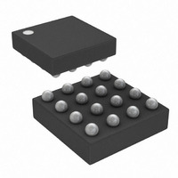
IC LASR CTRLR 1CHAN 5.5V 16CSBGA
Manufacturer
Maxim Integrated Products
Type
Laser Diode Controller (Fiber Optic)r
Datasheet
1.DS1861E.pdf
(25 pages)
Specifications of DS1861B+
Number Of Channels
1
Voltage - Supply
2.85 V ~ 5.5 V
Current - Supply
5mA
Operating Temperature
-40°C ~ 95°C
Package / Case
16-CSBGA
Mounting Type
Surface Mount
Lead Free Status / RoHS Status
Lead free / RoHS Compliant


The following terminology is commonly used to
describe I
Master Device: The master device controls the slave
devices on the bus. The master device generates SCL
clock pulses, and start and stop conditions.
Slave Devices: Slave devices send and receive data
at the master’s request.
Bus Idle or Not Busy: Time between stop and start
conditions when both SDA and SCL are inactive and in
their logic-high states.
Start Condition: A start condition is generated by the
master to initiate a new data transfer with a slave.
Transitioning SDA from high to low while SCL remains
high generates a start condition. See the timing dia-
gram for applicable timing.
Stop Condition: A stop condition is generated by the
master to end a data transfer with a slave. Transitioning
SDA from low to high while SCL remains high gener-
ates a stop condition. See the timing diagram for
applicable timing.
Repeated Start Condition: The master can use a
repeated start condition at the end of one data transfer to
indicate that it will immediately initiate a new data trans-
fer following the current one. Repeated starts are com-
monly used during read operations to identify a specific
memory address to begin a data transfer. A repeated
Figure 14. I
SDA
SCL
NOTE: TIMING IS REFERENCE TO V
STOP
2
2
C data transfers.
C Timing Diagram
t
BUF
Full Laser Control with Fault Management
START
IL(MAX)
t
t
HD:STA
LOW
AND V
IH(MIN)
.
I
t
2
R
____________________________________________________________________
t
HD:DAT
C Definitions
t
F
t
HIGH
t
SU:DAT
start condition is issued identically to a normal start con-
dition. See the timing diagram for applicable timing.
Bit Write: Transitions of SDA must occur during the low
state of SCL. The data on SDA must remain valid and
unchanged during the entire high pulse of SCL plus the
setup and hold time requirements (Figure 14). Data is
shifted into the device during the rising edge of the SCL.
Bit Read: At the end of a write operation, the master
must release the SDA bus line for the proper amount of
setup time (Figure 14) before the next rising edge of
SCL during a bit read. The device shifts out each bit of
data on SDA at the falling edge of the previous SCL
pulse and the data bit is valid at the rising edge of the
current SCL pulse. Remember that the master gener-
ates all SCL clock pulses including when it is reading
bits from the slave.
Acknowledgement
Acknowledgement (ACK) or Not Acknowledge (NACK)
is always the 9th bit transmitted during a byte transfer.
The device receiving data (the master during a read or
the slave during a write operation) performs an ACK by
transmitting a zero during the 9th bit. A device per-
forms a NACK by transmitting a one during the 9th bit.
Timing (Figure 14) for the ACK and NACK is identical to
all other bit writes. An ACK is the acknowledgment that
the device is properly receiving data. A NACK is used
to terminate a read sequence or as an indication that
the device is not receiving data.
REPEATED
START
t
SU:STA
t
HD:STA
(ACK
and
t
SP
NACK):
t
SU:STO
An
21
Related parts for DS1861B+
Image
Part Number
Description
Manufacturer
Datasheet
Request
R

Part Number:
Description:
Ds1861 Full Laser Control With Fault Management
Manufacturer:
Maxim Integrated Products, Inc.
Datasheet:

Part Number:
Description:
MAX7528KCWPMaxim Integrated Products [CMOS Dual 8-Bit Buffered Multiplying DACs]
Manufacturer:
Maxim Integrated Products
Datasheet:
Part Number:
Description:
Single +5V, fully integrated, 1.25Gbps laser diode driver.
Manufacturer:
Maxim Integrated Products
Datasheet:
Part Number:
Description:
Single +5V, fully integrated, 155Mbps laser diode driver.
Manufacturer:
Maxim Integrated Products
Datasheet:
Part Number:
Description:
VRD11/VRD10, K8 Rev F 2/3/4-Phase PWM Controllers with Integrated Dual MOSFET Drivers
Manufacturer:
Maxim Integrated Products
Datasheet:
Part Number:
Description:
Highly Integrated Level 2 SMBus Battery Chargers
Manufacturer:
Maxim Integrated Products
Datasheet:
Part Number:
Description:
Current Monitor and Accumulator with Integrated Sense Resistor; ; Temperature Range: -40°C to +85°C
Manufacturer:
Maxim Integrated Products
Part Number:
Description:
TSSOP 14/A�/RS-485 Transceivers with Integrated 100O/120O Termination Resis
Manufacturer:
Maxim Integrated Products
Part Number:
Description:
TSSOP 14/A�/RS-485 Transceivers with Integrated 100O/120O Termination Resis
Manufacturer:
Maxim Integrated Products
Part Number:
Description:
QFN 16/A�/AC-DC and DC-DC Peak-Current-Mode Converters with Integrated Step
Manufacturer:
Maxim Integrated Products
Part Number:
Description:
TDFN/A/65V, 1A, 600KHZ, SYNCHRONOUS STEP-DOWN REGULATOR WITH INTEGRATED SWI
Manufacturer:
Maxim Integrated Products
Part Number:
Description:
Integrated Temperature Controller f
Manufacturer:
Maxim Integrated Products
Part Number:
Description:
SOT23-6/I�/45MHz to 650MHz, Integrated IF VCOs with Differential Output
Manufacturer:
Maxim Integrated Products
Part Number:
Description:
SOT23-6/I�/45MHz to 650MHz, Integrated IF VCOs with Differential Output
Manufacturer:
Maxim Integrated Products
Part Number:
Description:
EVALUATION KIT/2.4GHZ TO 2.5GHZ 802.11G/B RF TRANSCEIVER WITH INTEGRATED PA
Manufacturer:
Maxim Integrated Products