DS1861B+ Maxim Integrated Products, DS1861B+ Datasheet - Page 12
DS1861B+
Manufacturer Part Number
DS1861B+
Description
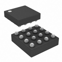
IC LASR CTRLR 1CHAN 5.5V 16CSBGA
Manufacturer
Maxim Integrated Products
Type
Laser Diode Controller (Fiber Optic)r
Datasheet
1.DS1861E.pdf
(25 pages)
Specifications of DS1861B+
Number Of Channels
1
Voltage - Supply
2.85 V ~ 5.5 V
Current - Supply
5mA
Operating Temperature
-40°C ~ 95°C
Package / Case
16-CSBGA
Mounting Type
Surface Mount
Lead Free Status / RoHS Status
Lead free / RoHS Compliant


Full Laser Control with Fault Management
The DS1861 APC is accomplished by adjusting the
bias current (I
from a photodiode matches the value determined by
the APC register. The relationship between the APC
register and I
where APC<4:0> is the numerical value determined by
the five least significant bits of the APC register, and
the gain value is determined by the upper three bits of
the APC register, as shown in the truth table below. See
Figure 7 for a graph of the BMD current-set point vs.
the APC register value.
12
____________________________________________________________________
TX-D
TX-F
GND
SDA
SCL
V
I
CC
A
APC<7:5>
A
A
SET
2
1
0
000
001
010
011
1xx
BMD
= 1.525µA Gain (APC<4:0> + 32)
BIAS
is given by:
) until the feedback current (I
Detailed Description
V
Automatic Power Control
CC
I
WITH SETTINGS
2
C-COMPATIBLE
PROTECTION
USER EEPROM
PASSWORD
INTERFACE
(8 BYTES)
DS1861
GAIN
16
1
2
4
8
FAULT MONITOR
NONVOLATILE
QUICK TRIP
BMD
POWER CONTROL
RATIO CONTROL
DISTURBANCE
NONVOLATILE
NONVOLATILE
AUTOMATIC
AUTOMATIC
EXTINCTION
)
CURRENT
The BMD pin appears to the photodiode as a voltage
source (V
in parallel with a current source (I
setpoint. When the control loop is at its steady state
value, the voltage at the BMD pin (V
V
When an imbalance causes the feedback current to differ
from the set current, the difference in the currents causes
the DS1861 to adjust the BIASSET and the MODSET cur-
rents to new settings so the input current matches the
set current. During transient periods, the difference in
the I
pass through R
decrease in the V
sink and source current, which must be configured using
the DPOL bit in the control byte for proper operation.
This allows the photodiode to be referenced to either
V
Register Descriptions sections for more detail.
REF
CC
I
I
B
BMD
V
CC
SET
, and the BMD current will all be sourced by I
or GND. See the Memory Map and Detailed
I
I
I
I
DIST
BMD
BMD
B
SINK/SOURCE
and I
REF
CURRENT
I
SET
) with an output resistance equal to R
BMD
BMD
BMD
V
currents causes a small current to
REF
. This causes a slight increase or
R
Σ
voltage. The current source can
BMD
Functional Diagram
CURRENT
SENSE
SET
) equal to the I
BMD
) is equal to
MODSET
BMD
BIASSET
BMD
BMD
SET
.
Related parts for DS1861B+
Image
Part Number
Description
Manufacturer
Datasheet
Request
R

Part Number:
Description:
Ds1861 Full Laser Control With Fault Management
Manufacturer:
Maxim Integrated Products, Inc.
Datasheet:

Part Number:
Description:
MAX7528KCWPMaxim Integrated Products [CMOS Dual 8-Bit Buffered Multiplying DACs]
Manufacturer:
Maxim Integrated Products
Datasheet:
Part Number:
Description:
Single +5V, fully integrated, 1.25Gbps laser diode driver.
Manufacturer:
Maxim Integrated Products
Datasheet:
Part Number:
Description:
Single +5V, fully integrated, 155Mbps laser diode driver.
Manufacturer:
Maxim Integrated Products
Datasheet:
Part Number:
Description:
VRD11/VRD10, K8 Rev F 2/3/4-Phase PWM Controllers with Integrated Dual MOSFET Drivers
Manufacturer:
Maxim Integrated Products
Datasheet:
Part Number:
Description:
Highly Integrated Level 2 SMBus Battery Chargers
Manufacturer:
Maxim Integrated Products
Datasheet:
Part Number:
Description:
Current Monitor and Accumulator with Integrated Sense Resistor; ; Temperature Range: -40°C to +85°C
Manufacturer:
Maxim Integrated Products
Part Number:
Description:
TSSOP 14/A�/RS-485 Transceivers with Integrated 100O/120O Termination Resis
Manufacturer:
Maxim Integrated Products
Part Number:
Description:
TSSOP 14/A�/RS-485 Transceivers with Integrated 100O/120O Termination Resis
Manufacturer:
Maxim Integrated Products
Part Number:
Description:
QFN 16/A�/AC-DC and DC-DC Peak-Current-Mode Converters with Integrated Step
Manufacturer:
Maxim Integrated Products
Part Number:
Description:
TDFN/A/65V, 1A, 600KHZ, SYNCHRONOUS STEP-DOWN REGULATOR WITH INTEGRATED SWI
Manufacturer:
Maxim Integrated Products
Part Number:
Description:
Integrated Temperature Controller f
Manufacturer:
Maxim Integrated Products
Part Number:
Description:
SOT23-6/I�/45MHz to 650MHz, Integrated IF VCOs with Differential Output
Manufacturer:
Maxim Integrated Products
Part Number:
Description:
SOT23-6/I�/45MHz to 650MHz, Integrated IF VCOs with Differential Output
Manufacturer:
Maxim Integrated Products
Part Number:
Description:
EVALUATION KIT/2.4GHZ TO 2.5GHZ 802.11G/B RF TRANSCEIVER WITH INTEGRATED PA
Manufacturer:
Maxim Integrated Products