MM74C926N Fairchild Semiconductor, MM74C926N Datasheet - Page 4
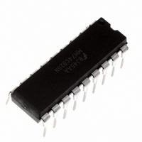
MM74C926N
Manufacturer Part Number
MM74C926N
Description
IC COUNTER 4DIG 7SEG DRVR 18-DIP
Manufacturer
Fairchild Semiconductor
Datasheet
1.MM74C928N.pdf
(9 pages)
Specifications of MM74C926N
Display Type
LED
Configuration
7 Segment
Interface
BCD
Digits Or Characters
4 Digits
Current - Supply
20µA
Voltage - Supply
3 V ~ 6 V
Operating Temperature
-40°C ~ 85°C
Mounting Type
Through Hole
Package / Case
18-DIP (0.300", 7.62mm)
Lead Free Status / RoHS Status
Lead free / RoHS Compliant
Other names
74C926
74C926N
74C926N
Available stocks
Company
Part Number
Manufacturer
Quantity
Price


www.fairchildsemi.com
CMOS TO CMOS
V
V
V
V
I
I
I
CMOS/LPTTL INTERFACE
V
V
V
V
OUTPUT DRIVE
V
R
I
I
IN(1)
IN(0)
CC
SOURCE
SINK
jA
Absolute Maximum Ratings
DC Electrical Characteristics
Min/Max limits apply at 40 C
Note 2:
IN(1)
IN(0)
OUT(1)
OUT(0)
IN(1)
IN(0)
OUT(1)
OUT(0)
OUT
ON
I
Symbol
Voltage at Any Output Pin
Voltage at Any Input Pin
Operating Temperature
Storage Temperature
Range
Power Dissipation (P
SOURCE
Range (T
jA
measured in free-air with device soldered into printed circuit board.
Logical “1” Input Voltage
Logical “0” Input Voltage
Logical “1” Output Voltage
(Carry-Out and Digit Output
Only)
Logical “0” Output Voltage
Logical “1” Input Current
Logical “0” Input Current
Supply Current
Logical “1” Input Voltage
Logical “0” Input Voltage
Logical “1” Output Voltage
(Carry-Out and Digit
Output Only)
Logical “0” Output Voltage
Output Voltage (Segment
Sourcing Output)
Output Resistance (Segment
Sourcing Output)
Output Resistance (Segment
Output) Temperature Coefficient
Output Source Current
(Digit Output)
Output Source Current
(Carry-Out)
Output Sink Current
(All Outputs)
Thermal Resistance
A
)
D
Parameter
)
t
j
Refer to P
85 C, unless otherwise noted
GND
GND
D(MAX)
0.3V to V
65 C to 150 C
40 C to 85 C
V
V
V
V
V
V
V
V
V
V
V
I
V
I
I
V
V
V
MM74C925: (Note 2)
MM74C926, MM74C927, MM74C928
O
OUT
I
OUT
I
(Note 1)
0.3V to 15V
OUT
OUT
CC
CC
CC
CC
CC
CC
CC
IN
CC
CC
CC
CC
CC
CC
CC
vs T
CC
360 A
0V or 5V
5V
5V
5V, I
5V, I
5V, V
5V, V
5V, Outputs Open Circuit,
4.75V
4.75V
4.75V,
4.75V, I
4.75V, V
5V, V
5V, V
A
65 mA, V
65 mA, V
40 mA, V
40 mA, V
Graph
0.3V
O
O
IN
IN
OUT
OUT
Conditions
O
10 A
OUT
10 A
15V
0V
CC
CC
360 A
CC
CC
0V, T
V
4
CC
Note 1: “Absolute Maximum Ratings” are those values beyond which the
safety of the device cannot be guaranteed. Except for “Operating Tempera-
ture Range” they are not meant to imply that the devices should be oper-
ated at these limits. The Electrical Characteristics table provides conditions
for actual device operation.
1.75V, T
Operating V
V
Lead Temperature
, T
5V, T
5V, T
5V T
5V T
j
CC
(Soldering, 10 seconds)
j
25 C
j
j
25 C
T
T
j
j
j
25 C
25 C
j
j
100 C
100 C
150 C
150 C
150 C
CC
Range
V
V
V
V
CC
CC
CC
CC
1.75
Min
3.5
4.5
2.4
1.75
1
1
1.6
2
2
2
V
V
V
CC
CC
CC
0.005
0.005
Typ
0.6
3.6
20
20
30
35
75
70
3.3
2
1.3
1.2
1.4
1000
Max
100
1.5
0.5
0.8
0.4
0.8
32
40
50
90
1
3V to 6V
260 C
Units
%/ C
6.5V
mA
mA
mA
C/W
C/W
V
V
V
V
V
V
V
V
V
V
V
A
A
A
Related parts for MM74C926N
Image
Part Number
Description
Manufacturer
Datasheet
Request
R

Part Number:
Description:
Fairchild Semiconductor [IGBT MODULE]
Manufacturer:
Fairchild Semiconductor
Datasheet:

Part Number:
Description:
Discrete Semiconductor Modules
Manufacturer:
Fairchild Semiconductor
Part Number:
Description:
Discrete Semiconductor Modules
Manufacturer:
Fairchild Semiconductor
Part Number:
Description:
This N-Channel MOSFET is produced using Fairchild Semiconductor’s advanced Power Trench® process
Manufacturer:
Fairchild Semiconductor
Datasheet:
Part Number:
Description:
This N-Channel MOSFET is produced using Fairchild Semiconductor’s advanced Power Trench® process
Manufacturer:
Fairchild Semiconductor
Datasheet:
Part Number:
Description:
This N-Channel MOSFET is produced using Fairchild Semiconductor’s advanced PowerTrench® process
Manufacturer:
Fairchild Semiconductor
Datasheet:
Part Number:
Description:
This N-Channel MOSFET is produced using Fairchild Semiconductor’s advanced PowerTrench® process
Manufacturer:
Fairchild Semiconductor
Datasheet:
Part Number:
Description:
This N-Channel MOSFET is produced using Fairchild Semiconductor’s advanced Power Trench® process
Manufacturer:
Fairchild Semiconductor
Datasheet:
Part Number:
Description:
This N-Channel logic Level MOSFETs are produced using Fairchild Semiconductor‘s advanced Power Trench® process that has been special tailored to minimize the on-state resistance and yet maintain superior switching performance
Manufacturer:
Fairchild Semiconductor
Datasheet:
Part Number:
Description:
This N-Channel MOSFET is produced using Fairchild Semiconductor’s advanced Power Trench® process
Manufacturer:
Fairchild Semiconductor
Datasheet:
Part Number:
Description:
This N-Channel SyncFET™ is produced using Fairchild Semiconductor’s advanced PowerTrench® process
Manufacturer:
Fairchild Semiconductor
Datasheet:
Part Number:
Description:
This N-Channel SyncFET™ is produced using Fairchild Semiconductor’s advanced PowerTrench® process
Manufacturer:
Fairchild Semiconductor
Datasheet:
Part Number:
Description:
This N-Channel SyncFET™ is produced using Fairchild Semiconductor’s advanced PowerTrench® process
Manufacturer:
Fairchild Semiconductor
Datasheet:
Part Number:
Description:
This N-Channel logic Level MOSFETs are produced using Fairchild Semiconductor‘s advanced Power Trench® process that has been special tailored to minimize the on-state resistance and yet maintain superior switching performance
Manufacturer:
Fairchild Semiconductor
Datasheet:
Part Number:
Description:
This N-Channel MOSFET is produced using Fairchild Semiconductor’s advanced Power Trench® process that has been especially tailored to minimize the on-state resistance and yet maintain superior switching performance
Manufacturer:
Fairchild Semiconductor
Datasheet: