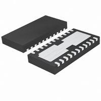
LTC4090EDJC#PBF Linear Technology, LTC4090EDJC#PBF Datasheet - Page 9

LTC4090EDJC#PBF
Manufacturer Part Number
LTC4090EDJC#PBF
Description
IC USB POWER MANAGER 22-DFN
Manufacturer
Linear Technology
Datasheet
1.LTC4090EDJCPBF.pdf
(28 pages)
Specifications of LTC4090EDJC#PBF
Function
Power Management
Battery Type
Lithium-Ion (Li-Ion), Lithium-Polymer (Li-Pol)
Voltage - Supply
4.35 V ~ 5.5 V
Operating Temperature
-40°C ~ 85°C
Mounting Type
Surface Mount
Package / Case
22-WFDFN Exposed Pad
Supply Voltage Range
4.35V To 5.5V
Operating Temperature Range
-40°C To +85°C
Digital Ic Case Style
DFN
No. Of Pins
22
Msl
MSL 1 - Unlimited
Termination Type
SMD
Supply Voltage Min
4.35V
Rohs Compliant
Yes
Filter Terminals
SMD
Frequency
2.7MHz
Lead Free Status / RoHS Status
Lead free / RoHS Compliant
Available stocks
Company
Part Number
Manufacturer
Quantity
Price
PIN FUNCTIONS
SYNC (Pin 1): External Clock Synchronization Input. See
synchronizing section in the Applications Information
section. Ground pin when not used.
PG (Pin 2): Open Collector Output of an Internal Compara-
tor. PG remains low until the HVOUT pin is above 2.8V.
PG output is valid when HVIN is above 3.6V and HVEN
is high.
R
to ground from this pin sets the switching frequency.
V
voltage on this pin controls the peak switch current in the
high voltage regulator. Tie an RC network from this pin to
ground to compensate the control loop.
NTC (Pin 5): Input to the NTC Thermistor Monitoring
Circuits. The NTC pin connects to a negative temperature
coeffi cient thermistor which is typically co-packaged with
the battery pack to determine if the battery is too hot or too
cold to charge. If the battery temperature is out of range,
charging is paused until the battery temperature re-enters
the valid range. A low drift bias resistor is required from
VNTC to NTC and a thermistor is required from NTC to
ground. If the NTC function is not desired, the NTC pin
should be grounded.
VNTC (Pin 6): Output Bias Voltage for NTC. A resistor from
this pin to the NTC pin will bias the NTC thermistor.
HVPR (Pin 7): High Voltage Present Output (Active Low).
A low on this pin indicates that the high voltage regulator
has suffi cient voltage to charge the battery. This feature
is enabled if power is present on HVIN, IN, or BAT (i.e.,
above UVLO thresholds).
CHRG (Pin 8): Open-Drain Charge Status Output. When
the battery is being charged, the CHRG pin is pulled low by
an internal N-channel MOSFET. When the timer runs out or
the charge current drops below 10% of the programmed
charge current or the input supply is removed, the CHRG
pin is forced to a high impedance state.
T
C
(Pin 3): Oscillator Resistor Input. Connecting a resistor
(Pin 4): High Voltage Buck Regulator Control Pin. The
PROG (Pin 9): Charge Current Program Pin. Connecting
a resistor from PROG to ground programs the charge
current:
GATE (Pin 10): External Ideal Diode Gate Connection. This
pin controls the gate of an optional external P-channel
MOSFET transistor used to supplement the internal ideal
diode. The source of the P-channel MOSFET should be
connected to OUT and the drain should be connected to
BAT. When not in use, this pin should be left fl oating. It
is important to maintain high impedance on this pin and
minimize all leakage paths.
BAT (Pin 11): Single-Cell Li-Ion Battery. This pin is used
as an output when charging the battery and as an input
when supplying power to OUT. When the OUT pin potential
drops below the BAT pin potential, an ideal diode function
connects BAT to OUT and prevents OUT from dropping
more than 100mV below BAT. A precision internal resistor
divider sets the fi nal fl oat (charging) potential on this pin.
The internal resistor divider is disconnected when IN and
HVIN are in undervoltage lockout.
IN (Pin 12): Input Supply. Connect to USB supply, V
Input current to this pin is limited to either 20% or 100%
of the current programmed by the CLPROG pin as deter-
mined by the state of the HPWR pin. Charge current (to the
BAT pin) supplied through the input is set to the current
programmed by the PROG pin but will be limited by the
input current limit if charge current is set greater than the
input current limit or if the sum of charge current plus load
current is greater than the input current limit.
OUT (Pin 13): Voltage Output. This pin is used to provide
controlled power to a USB device from either USB V
(IN), an external high voltage supply (HVIN), or the battery
(BAT) when no other supply is present. The high voltage
supply is prioritized over the USB V
be bypassed with at least 4.7μF to GND.
I
CHG
(A) =
50,000V
R
LTC4090/LTC4090-5
PROG
BUS
input. OUT should
BUS
4090fc
9
BUS
.


