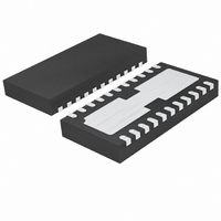
LTC4090EDJC#PBF Linear Technology, LTC4090EDJC#PBF Datasheet - Page 21

LTC4090EDJC#PBF
Manufacturer Part Number
LTC4090EDJC#PBF
Description
IC USB POWER MANAGER 22-DFN
Manufacturer
Linear Technology
Datasheet
1.LTC4090EDJCPBF.pdf
(28 pages)
Specifications of LTC4090EDJC#PBF
Function
Power Management
Battery Type
Lithium-Ion (Li-Ion), Lithium-Polymer (Li-Pol)
Voltage - Supply
4.35 V ~ 5.5 V
Operating Temperature
-40°C ~ 85°C
Mounting Type
Surface Mount
Package / Case
22-WFDFN Exposed Pad
Supply Voltage Range
4.35V To 5.5V
Operating Temperature Range
-40°C To +85°C
Digital Ic Case Style
DFN
No. Of Pins
22
Msl
MSL 1 - Unlimited
Termination Type
SMD
Supply Voltage Min
4.35V
Rohs Compliant
Yes
Filter Terminals
SMD
Frequency
2.7MHz
Lead Free Status / RoHS Status
Lead free / RoHS Compliant
Available stocks
Company
Part Number
Manufacturer
Quantity
Price
APPLICATIONS INFORMATION
High Voltage Regulator Frequency Compensation
The LTC4090/LTC4090-5 high voltage regulator uses
current mode control to regulate the output. This simpli-
fi es loop compensation. In particular, the high voltage
regulator does not require the ESR of the output capacitor
for stability, so you are free to use ceramic capacitors to
achieve low output ripple and small circuit size. Frequency
compensation is provided by the components tied to the
V
and a resistor (R
dition, there may be a lower value capacitor in parallel.
This capacitor (C
but is used to fi lter noise at the switching frequency, and
is required only if a phase-lead capacitor is used or if the
output capacitor has high ESR.
Loop compensation determines the stability and transient
performance. Designing the compensation network is a bit
complicated and the best values depend on the application
and in particular the type of output capacitor. A practical
approach is to start with the front page schematic and tune
the compensation network to optimize performance. Stabil-
ity should then be checked across all operating conditions,
including load current, input voltage and temperature. The
LTC1375 data sheet contains a more thorough discussion
of loop compensation and describes how to test the sta-
bility using a transient load. Figure 5 shows the transient
response when the load current is stepped from 500mA
to 1500mA and back to 500mA.
C
pin, as shown in Figure 1. Generally a capacitor (C
Figure 5. Transient Load Response of the LTC4090 High
Voltage Regulator Front Page Application as the Load
Current is Stepped from 500mA to 1500mA.
50mV/DIV
HVOUT
1A/DIV
I
L
FIGURE 12 SCHEMATIC
F
C
) is not part of the loop compensation
) in series to ground are used. In ad-
25μs/DIV
4090 F05
C
)
Low Ripple Burst Mode Operation and
Pulse-Skipping Mode
The LTC4090/LTC4090-5 are capable of operating in either
low ripple Burst Mode operation or pulse-skipping mode
which are selected using the SYNC pin. Tie the SYNC pin
below V
operation or above V
skipping mode.
To enhance effi ciency at light loads, the LTC4090/LTC4090-5
can be operated in low ripple Burst Mode operation which
keeps the output capacitor charged to the proper voltage
while minimizing the input quiescent current. During Burst
Mode operation, the LTC4090/LTC4090-5 deliver single
cycle bursts of current to the output capacitor followed
by sleep periods where the output power is delivered to
the load by the output capacitor. Because the LTC4090/
LTC4090-5 deliver power to output with single, low current
pulses, the output ripple is kept below 15mV for a typical
application. As the load current decreases towards a no
load condition, the percentage of time that the high volt-
age regulator operates in sleep mode increases and the
average input current is greatly reduced resulting in high
effi ciency even at very low loads. See Figure 6.
At higher output loads (above 70mA for the front page
application) the LTC4090/LTC4090-5 will be running at
the frequency programmed by the R
operating in standard PWM mode. The transition between
PWM and low ripple Burst Mode operation is seamless,
and will not disturb the output voltage.
Figure 6. High Voltage Regulator Burst Mode Operation
SYNC,L
10mV/DIV
0.5A/DIV
5V/DIV
V
V
OUT
SW
I
L
(typically 0.5V) for low ripple Burst Mode
V
I
LTC4090/LTC4090-5
LOAD
IN
= 12V; FIGURE 12 SCHEMATIC
= 10mA
SYNC,H
5μs/DIV
(typically 0.8V) for pulse-
T
resistor, and will be
4090 F06
21
4090fc


