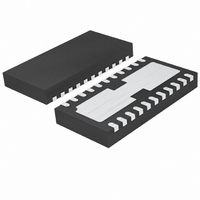
LTC4090EDJC#PBF Linear Technology, LTC4090EDJC#PBF Datasheet - Page 10

LTC4090EDJC#PBF
Manufacturer Part Number
LTC4090EDJC#PBF
Description
IC USB POWER MANAGER 22-DFN
Manufacturer
Linear Technology
Datasheet
1.LTC4090EDJCPBF.pdf
(28 pages)
Specifications of LTC4090EDJC#PBF
Function
Power Management
Battery Type
Lithium-Ion (Li-Ion), Lithium-Polymer (Li-Pol)
Voltage - Supply
4.35 V ~ 5.5 V
Operating Temperature
-40°C ~ 85°C
Mounting Type
Surface Mount
Package / Case
22-WFDFN Exposed Pad
Supply Voltage Range
4.35V To 5.5V
Operating Temperature Range
-40°C To +85°C
Digital Ic Case Style
DFN
No. Of Pins
22
Msl
MSL 1 - Unlimited
Termination Type
SMD
Supply Voltage Min
4.35V
Rohs Compliant
Yes
Filter Terminals
SMD
Frequency
2.7MHz
Lead Free Status / RoHS Status
Lead free / RoHS Compliant
Available stocks
Company
Part Number
Manufacturer
Quantity
Price
LTC4090/LTC4090-5
PIN FUNCTIONS
CLPROG (Pin 14): Current Limit Program and Input Cur-
rent Monitor. Connecting a resistor, R
programs the input to output current limit. The current
limit is programmed as follows:
In USB applications, the resistor R
to no less than 2.1k. The voltage on the CLPROG pin is
always proportional to the current fl owing through the
IN to OUT power path. This current can be calculated as
follows:
HPWR (Pin 15): High Power Select. This logic input is used
to control the input current limit. A voltage greater than
1.2V on the pin will set the input current limit to 100% of
the current programmed by the CLPROG pin. A voltage
less than 0.4V on the pin will set the input current limit to
20% of the current programmed by the CLPROG pin. A
2μA pull-down current is internally connected to this pin
to ensure it is low at power up when the pin is not being
driven externally.
SUSP (Pin 16): Suspend Mode Input. Pulling this pin
above 1.2V will disable the power path from IN to OUT.
The supply current from IN will be reduced to comply
with the USB specifi cation for suspend mode. Both the
ability to charge the battery from HVIN and the ideal diode
function (from BAT to OUT) will remain active. Suspend
mode will reset the charge timer if OUT is less than BAT
while in suspend mode. If OUT is kept greater than BAT,
such as when the high voltage input is present, the charge
timer will not be reset when the part is put in suspend. A
2μA pull-down current is internally connected to this pin
to ensure it is low at power up when the pin is not being
driven externally.
TIMER (Pin 17): Timer Capacitor. Placing a capacitor,
C
is:
10
TIMER
I
I
t
CL
IN
TIMER
(A) =
(A) =
, to GND sets the timer period. The timer period
(hours) =
R
R
V
1000V
CLPROG
CLPROG
CLPROG
C
• 1000
TIMER
0.1µF • 100k
• R
PROG
CLPROG
• 3hours
CLPROG
should be set
, to ground
Charge time is increased if charge current is reduced
due to load current, thermal regulation and current limit
selection (HPWR low).
Shorting the TIMER pin to GND disables the battery
charging functions.
HVOUT (Pin 18): Voltage Output of the High Voltage
Regulator. When suffi cient voltage is present at HVOUT,
the low voltage power path from IN to OUT will be discon-
nected and the HVPR pin will be pulled low to indicate
that a high voltage wall adapter has been detected. The
LTC4090 high voltage regulator will maintain just enough
differential voltage between HVOUT and BAT to keep the
battery charger MOSFET out of dropout (typically 300mV
from OUT to BAT). The LTC4090-5 high voltage regulator
will provide a 5V output to the battery charger MOSFET.
HVOUT should be bypassed with at least 22μF to GND.
BOOST (Pin 19): This pin is used to provide drive voltage,
higher than the input voltage, to the internal bipolar NPN
power switch.
SW (Pin 20): The SW pin is the output of the internal high
voltage power switch. Connect this pin to the inductor,
catch diode and boost capacitor.
HVIN (Pin 21): High Voltage Regulator Input. The HVIN pin
supplies current to the internal high voltage regulation and
to the internal high voltage power switch. The presence
of a high voltage input takes priority over the USB V
input (i.e., when a high voltage input supply is detected,
the USB IN to OUT path is disconnected). This pin must
be locally bypassed.
HVEN (Pin 22): High Voltage Regulator Enable Input. The
HVEN pin is used to disable the high voltage input path.
Tie to ground to disable the high voltage input or tie to at
least 2.3V to enable the high voltage path. If this feature
is not used, tie HVEN to the HVIN pin. This pin can also
be used to soft-start the high voltage regulator; see the
Applications Information section for more information.
Exposed Pad (Pin 23): Ground. The exposed package pad
is ground and must be soldered to the PC board for proper
functionality and for maximum heat transfer (use several
vias directly under the LTC4090/LTC4090-5).
4090fc
BUS


