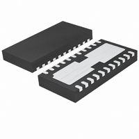
LTC4090EDJC#PBF Linear Technology, LTC4090EDJC#PBF Datasheet - Page 14

LTC4090EDJC#PBF
Manufacturer Part Number
LTC4090EDJC#PBF
Description
IC USB POWER MANAGER 22-DFN
Manufacturer
Linear Technology
Datasheet
1.LTC4090EDJCPBF.pdf
(28 pages)
Specifications of LTC4090EDJC#PBF
Function
Power Management
Battery Type
Lithium-Ion (Li-Ion), Lithium-Polymer (Li-Pol)
Voltage - Supply
4.35 V ~ 5.5 V
Operating Temperature
-40°C ~ 85°C
Mounting Type
Surface Mount
Package / Case
22-WFDFN Exposed Pad
Supply Voltage Range
4.35V To 5.5V
Operating Temperature Range
-40°C To +85°C
Digital Ic Case Style
DFN
No. Of Pins
22
Msl
MSL 1 - Unlimited
Termination Type
SMD
Supply Voltage Min
4.35V
Rohs Compliant
Yes
Filter Terminals
SMD
Frequency
2.7MHz
Lead Free Status / RoHS Status
Lead free / RoHS Compliant
Available stocks
Company
Part Number
Manufacturer
Quantity
Price
LTC4090/LTC4090-5
OPERATION
The oscillator reduces the switch regulator’s operating
frequency when the voltage at the HVOUT pin is low (be-
low 2.95V). This frequency foldback helps to control the
output current during start-up and overload.
The high voltage regulator contains a power good com-
parator which trips when the HVOUT pin is at 2.8V. The PG
output is an open-collector transistor that is off when the
output is in regulation, allowing an external resistor to pull
the PG pin high. Power good is valid when the switching
regulator is enabled and HVIN is above 3.6V.
Ideal Diode From BAT to OUT
The LTC4090/LTC4090-5 have an internal ideal diode as
well as a controller for an optional external ideal diode. If
a battery is the only power supply available, or if the load
current exceeds the programmed input current limit, then
the battery will automatically deliver power to the load via
an ideal diode circuit between the BAT and OUT pins. The
ideal diode circuit (along with the recommended 4.7μF
capacitor on the OUT pin) allows the LTC4090/LTC4090-5
to handle large transient loads and wall adapter or USB
V
large bulk capacitors. The ideal diode responds within
a few microseconds and prevents the OUT pin voltage
from dropping signifi cantly below the BAT pin voltage.
14
4090 F02a
BUS
500
400
300
200
100
(a) High Power Mode/Full Charge
R
0
PROG
0
connect/disconnect scenarios without the need for
= 100k and R
100
200
I
LOAD(mA)
300
(CHARGING)
CLPROG
I
BAT
I
LOAD
400
(IDEAL DIODE)
I
IN
= 2k
500
I
Figure 2. Input and Battery Currents as a Function of Load Current
BAT
4090 F02b
100
80
60
40
20
0
(b) Low Power Mode/Full Charge
R
0
PROG
20
= 100k and R
40
I
LOAD(mA)
A comparison of the I-V curve of the ideal diode and a
Schottky diode can be seen in Figure 3.
If the desired input current increases beyond the pro-
grammed input current limit additional current will be drawn
from the battery via the internal ideal diode. Furthermore,
if power to IN (USB V
is removed, then all of the application power will be pro-
vided by the battery via the ideal diode. A 4.7μF capacitor
at OUT is suffi cient to keep a transition from input power
to battery power from causing signifi cant output voltage
droop. The ideal diode consists of a precision amplifi er that
enables a large P-channel MOSFET transistor whenever the
voltage at OUT is approximately 20mV (V
voltage at BAT. The resistance of the internal ideal diode
is approximately 215mΩ.
If this is suffi cient for the application then no external
components are necessary. However if more conductance
is needed, an external P-channel MOSFET can be added
from BAT to OUT. The GATE pin of the LTC4090/LTC4090-5
drives the gate of the external PFET for automatic ideal
diode control. The source of the external MOSFET should
be connected to OUT and the drain should be connected
to BAT. In order to help protect the external MOSFET in
overcurrent situations, it should be placed in close thermal
contact to the LTC4090/LTC4090-5.
60
(CHARGING)
CLPROG
I
BAT
I
LOAD
80
(IDEAL DIODE)
I
IN
= 2k
100
I
BAT
BUS
4090 F02c
500
400
300
200
100
0
) or HVIN (high voltage input)
0
(c) High Power Mode with
I
R
CL
PROG
I
BAT
= 500mA and I
100
= I
= 100k and R
CHG
200
I
IN
I
LOAD (mA)
300
(CHARGING)
FWD
CHG
I
BAT
I
CLPROG
I
LOAD
BAT
) below the
400
(IDEAL DIODE)
= 250mA
= I
CL
500
= I
= 2k
I
BAT
OUT
4090fc


