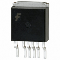
FS6X0720RJX Fairchild Semiconductor, FS6X0720RJX Datasheet

FS6X0720RJX
Specifications of FS6X0720RJX
Related parts for FS6X0720RJX
FS6X0720RJX Summary of contents
Page 1
... Part Number Range FS6X0420RJ -25°C to +85°C FS6X0720RJ -25°C to +85°C FS6X1220RJ -25°C to +85°C FS6X0420RJX -25°C to +85°C FS6X0720RJX -25°C to +85°C (2) FS6X1220RJX -25°C to +85°C Note Tape & Reel FPS is a trademark of Fairchild Semiconductor Corporation TM ©2006 Fairchild Semiconductor Corporation FS6X0420RJ/ FS6X0720RJ/ FS6X1220RJ Rev ...
Page 2
Typical Application Diagram DC IN Internal Block Diagram V LU Line 6 Sense ref I I delay OVP TSD Line UVLO Figure 2. Functional Block Diagram of ...
Page 3
Pin Assignments Pin Definitions Pin Number Pin Name 1 Drain 2 GND 3 Vcc Feedback 4 (FB) 5 N.C. 6 Line Sense (LS) FS6X0420RJ/ FS6X0720RJ/ FS6X1220RJ Rev. 1.0.1 D2-PAK-6L 6. Line Sense 5. N.C. 4. Vfb 3. Vcc 2. GND ...
Page 4
Absolute Maximum Ratings (Ta=25°C, unless otherwise specified Parameter Drain-source Voltage (1) Pulsed Drain Current (Tc=25°C) Continuous Drain Current (Tc=25°C) Continuous Drain Current (Tc=100°C) Supply Voltage Input Voltage Range Total Power Dissipation (Tc=25°C) Operating Junction Temperature Operating Ambient Temperature Storage Temperature ...
Page 5
Electrical Characteristics (Ta=25°C, unless otherwise specified.) Parameter SENSE FET SECTION Drain Source Breakdown Voltage Zero Gate Voltage Drain Current Static Drain Source on Resistance (1) Output Capacitance CONTROL SECTION Initial Frequency Voltage Stability (2) Temperature Stability Maximum Duty Cycle Minimum ...
Page 6
Electrical Characteristics (Ta=25°C, unless otherwise specified.) Parameter TOTAL DEVICE SECTION (1) Startup Current Sleep Mode Current (1) Operating Supply Current Line UVLO Threshold Voltage Sleep On/Off Threshold Voltage Notes: 1. This parameter is the current flowing into the control IC. ...
Page 7
Typical Performance Characteristics (These Characteristic Graphs are Normalized at Ta= 25°C.) [mA] 11.0 10.5 10.0 9.5 9.0 - Temp [℃] Figure 4. Operating Current vs. Temp [V] 9.50 9.25 9.00 8.75 8.50 - Temp ...
Page 8
Typical Performance Characteristics (Continued) (These Characteristic Graphs are Normalized at Ta= 25°C) [V] 7.60 7.55 7.50 7.45 7.40 - Temp [℃] Figure 10. Shutdown FB Voltage vs. Temp [V] 26.0 25.5 25.0 24.5 24.0 - ...
Page 9
Applications Information 1. Startup To guarantee stable operation of the control IC, Vcc has under voltage lockout (UVLO) with 6V hysteresis. Figure 16 shows the relation between the supply current (Icc) and the supply voltage (Vcc). Before Vcc reaches 15V, ...
Page 10
Over Load Protection (OLP) Overload means that the load current exceeds a pre-set level due to an abnormal situation. In this situation, the protection cir- cuit should be activated to protect the SMPS (Switch Mode Power Supplies). However, even ...
Page 11
Typical Application Circuit Application Output power PoE Device Features High switching frequency(300kHz) High power density Low component count Enhanced system reliability through various protection functions Key Design Notes Capacitor C104 is employed to reduce the noise on sensed line voltage. ...
Page 12
Transformer N Vcc N p/2 N s/2 N s/1 N p/1 3. Winding Specifications No Pin (s→f) 1 → 11 Np/1 Insulation: Polyester Tape t = 0.050mm, 2Layers 6 → 5 Ns/1 Insulation: Polyester Tape t = 0.050mm, 2Layers ...
Page 13
Demo Circuit Part List Part Value Resistor R101 200K R102 100K R104 1K R105 18K R210 40K R201 1K R211 1K R212 30K R213 18K R214 18K R221 15K R222 15K R223 15K R301 10K - - Diode D102 ...
Page 14
Mechanical Dimensions D2-Pak-6L FS6X0420RJ/ FS6X0720RJ/ FS6X1220RJ Rev. 1.0.1 14 Unit: mm www.fairchildsemi.com ...
Page 15
... TRADEMARKS The following are registered and unregistered trademarks Fairchild Semiconductor owns or is authorized to use and is not intended exhaustive list of all such trademarks. FAST ® ACEx™ ActiveArray™ FASTr™ Bottomless™ FPS™ Build it Now™ FRFET™ CoolFET™ ...


