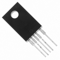
FSCQ0765RTYDTU Fairchild Semiconductor, FSCQ0765RTYDTU Datasheet - Page 14

FSCQ0765RTYDTU
Manufacturer Part Number
FSCQ0765RTYDTU
Description
IC SWIT PWM GREEN OVP HV TO220
Manufacturer
Fairchild Semiconductor
Datasheet
1.FSCQ0765RTYDTU.pdf
(45 pages)
Specifications of FSCQ0765RTYDTU
Output Isolation
Isolated
Frequency Range
18 ~ 22kHz
Voltage - Input
9 ~ 20 V
Voltage - Output
650V
Power (watts)
100W
Operating Temperature
25°C ~ 150°C
Package / Case
TO-220-5 Full Pack (Formed Leads)
Power Switch Family
FSCQ0765RT
Input Voltage
-0.3 to 20V
Power Switch On Resistance
1.4Ohm
Output Current
4.4A
Number Of Outputs
Single
Mounting
Through Hole
Supply Current
4mA
Package Type
TO-220F
Operating Temperature (min)
-25C
Operating Temperature (max)
85C
Operating Temperature Classification
Commercial
Pin Count
5 +Tab
Power Dissipation
45W
On Resistance (max)
1.4 Ohms
Maximum Operating Temperature
+ 85 C
Minimum Operating Temperature
- 25 C
Maximum Power Dissipation
45000 mW
Mounting Style
Through Hole
Supply Voltage (max)
20 V
No. Of Outputs
1
Power Dissipation Pd
85W
No. Of Pins
5
Operating Temperature Range
-25°C To +85°C
Filter Terminals
Through Hole
Ic Generic Number
0765
Rohs Compliant
Yes
Current Rating
5A
Frequency
20kHz
Lead Free Status / RoHS Status
Lead free / RoHS Compliant
Other names
FSCQ0765RTYDTU_NL
FSCQ0765RTYDTU_NL
FSCQ0765RTYDTU_NL
Available stocks
Company
Part Number
Manufacturer
Quantity
Price
Company:
Part Number:
FSCQ0765RTYDTU
Manufacturer:
FSC
Quantity:
20 000
Part Number:
FSCQ0765RTYDTU
Manufacturer:
FAIRCHILD/仙童
Quantity:
20 000
FSCQ-Series Rev. 1.1.2
Functional Description
1. Startup: Figure 4 shows the typical startup circuit and
the transformer auxiliary winding for the FSCQ-Series.
Before the FSCQ-Series begins switching, it consumes
only startup current (typically 25µA). The current sup-
plied from the AC line charges the external capacitor
(C
reaches the start voltage of 15V (V
Series begins switching, and its current consumption
increases to I
normal switching operation and the power required for
the FSCQ-Series is supplied from the transformer auxil-
iary winding, unless V
9V (V
control IC, V
6V hysteresis. Figure 5 shows the relationship between
the operating supply current of the FSCQ-Series and the
supply voltage (V
I
(V
START
a1
ac min
I
I
CC
OP
Figure 5. Relationship Between Operating
) that is connected to the Vcc pin. When Vcc
AC line
STOP
– V
FSCQ0565RT : 4mA (Typ.)
FSCQ0765RT : 4mA (Typ.)
FSCQ0965RT : 6mA (Typ.)
FSCQ1265RT : 6mA (Typ.)
FSCQ1465RT : 7mA (Typ.)
FSCQ1565RT : 7mA (Typ.)
FSCQ1565RP : 7mA (Typ.)
I
Supply Current and Vcc Voltage
Power Down
OP
ac max
FSCQ-Series
). To guarantee the stable operation of the
CC
Value
OP
Figure 4. Startup circuit
)
has under voltage lockout (UVLO) with
. Then, the FSCQ-Series continues its
CC
Vstop = 9V
).
CC
drops below the stop voltage of
V
CC
Rstr
Vstart = 15V
C
1N4007
I
sup
a1
Power Up
START
C
DC
), the FSCQ-
C
a2
Da
Vz
V
CC
14
The minimum average of the current supplied from the
AC is given by:
where V
FSCQ-Series start voltage
resistor. The startup resistor should be chosen so that
I
(50µA).
Once the resistor value is determined, the maximum loss
in the startup resistor is obtained as:
where V
resistor should have properly-rated dissipation wattage.
2. Synchronization: The FSCQ-Series employs a quasi-
resonant switching technique to minimize the switching
noise and loss. In this technique, a capacitor (Cr) is
added between the MOSFET drain and the source as
shown in Figure 6. The basic waveforms of the quasi-
resonant converter are shown in Figure 7. The external
capacitor lowers the rising slope of the drain voltage to
reduce the EMI caused when the MOSFET turns off. To
minimize the MOSFET’s switching loss, the MOSFET
should be turned on when the drain voltage reaches its
minimum value as shown in Figure 7.
Loss
sup
Sync
avg
C
DC
=
I
is larger than the maximum startup current
ac
ac
Figure 6. Synchronization Circuit
sup
C
--------- -
R
V
max
min
a1
1
CC
str
avg
V
+
–
DC
GND
Drain
is the minimum input voltage, V
is the maximum input voltage. The startup
=
R
---------------------------------------------- -
V
CC
C
C
ac
a2
---------------------------- -
SY
max 2
V
Ids
2 V
CO
Cr
2
ac
R
R
D
+
V
D
SY2
min
SY1
SY
+
–
(15V),
ds
V
a
start
–
Np
Lm
V
------------- -
Na
2
start
and R
2
–
2 2 V
---------------------------------------------------- -
Ns
str
--------- -
R
1
str
is the startup
www.fairchildsemi.com
start
start
V
is the
Vo
ac
max


