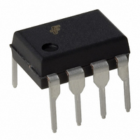
FSQ0370RNA Fairchild Semiconductor, FSQ0370RNA Datasheet - Page 12

FSQ0370RNA
Manufacturer Part Number
FSQ0370RNA
Description
IC SWIT PWM GREEN OVP UVLO 8DIP
Manufacturer
Fairchild Semiconductor
Series
FPS™r
Specifications of FSQ0370RNA
Output Isolation
Isolated
Frequency Range
92kHz ~ 108kHz
Voltage - Input
9 V ~ 20 V
Voltage - Output
700V
Power (watts)
27W
Operating Temperature
25°C ~ 140°C
Package / Case
8-DIP (0.300", 7.62mm)
Power Switch Family
FSQ0370
Power Switch On Resistance
4Ohm
Output Current
970mA
Number Of Outputs
Single
Mounting
Through Hole
Supply Current
3mA
Package Type
PDIP
Operating Temperature (min)
-25C
Operating Temperature (max)
85C
Operating Temperature Classification
Commercial
Pin Count
8
Power Dissipation
1.5W
On Resistance (max)
4 Ohms
Maximum Operating Temperature
+ 85 C
Minimum Operating Temperature
- 25 C
Maximum Power Dissipation
1500 mW
Mounting Style
Through Hole
Lead Free Status / RoHS Status
Lead free / RoHS Compliant
Available stocks
Company
Part Number
Manufacturer
Quantity
Price
Company:
Part Number:
FSQ0370RNA
Manufacturer:
FSC
Quantity:
81 000
Part Number:
FSQ0370RNA
Manufacturer:
FAIRCHILD/仙童
Quantity:
20 000
FSQ0170RNA, FSQ0270RNA, FSQ0370RNA Rev. 1.0.2
© 2006 Fairchild Semiconductor Corporation
Typical Application Circuit
Features
Key Design Notes
1. Schematic
Input
CON1
RL4
120k
1
2
3
KSP2907A
High efficiency (> 78% at 115 V
Low standby mode power consumption (< 0.8W at 230 V
Enhanced system reliability through various protection functions
Internal soft-start (10ms)
Line UVLO function can be achieved using external component
The delay time for overload protection is designed to be about 30ms with C8 of 47nF. If faster/slower triggering of
OLP is required, C8 can be changed to a smaller/larger value (e.g. 100nF for about 60ms).
ZP1, DL1, RL1, RL2, RL3, RL4, RL5, RL7, QL1, QL2, and CL9 build a Line Under-Voltage Lockout block (UVLO).
The Zener voltage of ZP1 determines the input voltage that makes FPS turn on. RL5 and DL1 provide a reference
voltage from V
QL2 turn on and pull down V
An evaluation board and corresponding test report can be provided.
RL2
1M
PC Auxiliary Power Supply
10μF
2.4 1W
CL9
50V
(Using FSQ0270RNA)
QL1
R6
RL3
1k
Application
1N5233B
RL7
40k
DL1
1N4007
RL1 1M
1N4007
KSP2222A
D2
D4
QL2
1N4007
1N4007
CC
open
J3
D3
D5
J2
0
30k
RL5
FOD817A
. If the input voltage divided by RL1, RL2, and RL4 is lower than the Zener voltage of DL1, QL1 and
U1B
4
3
22μF
400V
C2
0
L3
4.7k
R8
open
330μH
R2
L1
8 7 6 5
1 2 3 4
ZD2
open
FB
C8
47nF
U3
AC
22μF
400V
FSQ0270RNA
C3
to ground.
R13
open
Output power
and 230 V
ZR1
80
1N4745
ZD1
15W
1N4762
ZP1
1nF
250V
C10
FB
47μF
25V
Figure 21. Demo Circuit
J1
C7
AC
P6KE180A
input)
ZDS1
1N4007
R12
open
D6
R14
1N4007
30
DS1
R10
2
2.2nF
AC250V
12
C1
AC
3
Input Voltage
T1
1
EE2229
Universal input
4
5
(85-265 V
input and 0.5W load)
9,
6,
7
10
RS1
9
D1
SB540
1.5nF
CS1
AC
1000μF
16V
C4
)
1000μF
16V
C9
Output Voltage (Max. Current)
TL431A
U2
R3
560
1
2
3
2
U1A
FOD817A
100
R4
47nF
1
C6
10k
R9
5V (3A)
J4
0
FSQ0x70RNA Rev. 1.12
L2
1μH
1.25k
1%
1.2k
1%
R5
R11
www.fairchildsemi.com
470μF
10V
C5
CON2
Output
1
2


