FSQ0365RN Fairchild Semiconductor, FSQ0365RN Datasheet - Page 4
FSQ0365RN
Manufacturer Part Number
FSQ0365RN
Description
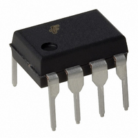
IC SWIT PWM GREEN OVP UVLO 8DIP
Manufacturer
Fairchild Semiconductor
Datasheet
1.FSQ0365RN.pdf
(24 pages)
Specifications of FSQ0365RN
Output Isolation
Isolated
Frequency Range
50.5 ~ 95.2kHz
Voltage - Input
8 ~ 20 V
Voltage - Output
650V
Power (watts)
25W
Operating Temperature
-40°C ~ 150°C
Package / Case
8-DIP (0.300", 7.62mm)
On Resistance (max)
4.5 Ohms
Maximum Operating Temperature
+ 85 C
Minimum Operating Temperature
- 25 C
Maximum Power Dissipation
1500 mW
Mounting Style
Through Hole
Supply Current
3 mA
Lead Free Status / RoHS Status
Lead free / RoHS Compliant
Available stocks
Company
Part Number
Manufacturer
Quantity
Price

Part Number:
FSQ0365RN
Manufacturer:
FARICHILD
Quantity:
20 000


FSQ0365, FSQ0265, FSQ0165, FSQ321, FSQ311 Rev. 1.0.5
© 2006 Fairchild Semiconductor Corporation
Pin Configuration
Pin Definitions
Pin #
6,7,8
1
2
3
4
5
Name
Drain
GND
Sync
Vcc
Vstr
Vfb
SenseFET source terminal on primary side and internal control ground.
Positive supply voltage input. Although connected to an auxiliary transformer winding, current
is supplied from pin 5 (Vstr) via an internal switch during startup (see Internal Block Diagram
Section). It is not until V
switch opens and device power is supplied via the auxiliary transformer winding.
The feedback voltage pin is the non-inverting input to the PWM comparator. It has a 0.9mA
current source connected internally while a capacitor and optocoupler are typically connected
externally. There is a time delay while charging external capacitor Cfb from 3V to 6V using an
internal 5μA current source. This time delay prevents false triggering under transient condi-
tions but still allows the protection mechanism to operate under true overload conditions.
This pin is internally connected to the sync-detect comparator for valley switching. Typically the
voltage of the auxiliary winding is used as Sync input voltage and external resistors and capac-
itor are needed to make time delay to match valley point. The threshold of the internal sync
comparator is 0.7V/0.2V.
This pin is connected to the rectified AC line voltage source. At start-up the internal switch sup-
plies internal bias and charges an external storage capacitor placed between the Vcc pin and
ground. Once the Vcc reaches 12V, the internal switch is opened.
The drain pins are designed to connect directly to the primary lead of the transformer and are
capable of switching a maximum of 700V. Minimizing the length of the trace connecting these
pins to the transformer will decrease leakage inductance.
Figure 3. Pin Configuration (Top View)
Sync
GND
Vcc
Vfb
CC
reaches the UVLO upper threshold (12V) that the internal start-up
FSQ0365RN Rev.01
8-LSOP
8-DIP
V
4
Description
Vstr
D
D
D
www.fairchildsemi.com
Related parts for FSQ0365RN
Image
Part Number
Description
Manufacturer
Datasheet
Request
R

Part Number:
Description:
Fairchild Semiconductor [IGBT MODULE]
Manufacturer:
Fairchild Semiconductor
Datasheet:

Part Number:
Description:
Discrete Semiconductor Modules
Manufacturer:
Fairchild Semiconductor
Part Number:
Description:
Discrete Semiconductor Modules
Manufacturer:
Fairchild Semiconductor
Part Number:
Description:
This N-Channel MOSFET is produced using Fairchild Semiconductor’s advanced Power Trench® process
Manufacturer:
Fairchild Semiconductor
Datasheet:
Part Number:
Description:
This N-Channel MOSFET is produced using Fairchild Semiconductor’s advanced Power Trench® process
Manufacturer:
Fairchild Semiconductor
Datasheet:
Part Number:
Description:
This N-Channel MOSFET is produced using Fairchild Semiconductor’s advanced PowerTrench® process
Manufacturer:
Fairchild Semiconductor
Datasheet:
Part Number:
Description:
This N-Channel MOSFET is produced using Fairchild Semiconductor’s advanced PowerTrench® process
Manufacturer:
Fairchild Semiconductor
Datasheet:
Part Number:
Description:
This N-Channel MOSFET is produced using Fairchild Semiconductor’s advanced Power Trench® process
Manufacturer:
Fairchild Semiconductor
Datasheet:
Part Number:
Description:
This N-Channel logic Level MOSFETs are produced using Fairchild Semiconductor‘s advanced Power Trench® process that has been special tailored to minimize the on-state resistance and yet maintain superior switching performance
Manufacturer:
Fairchild Semiconductor
Datasheet:
Part Number:
Description:
This N-Channel MOSFET is produced using Fairchild Semiconductor’s advanced Power Trench® process
Manufacturer:
Fairchild Semiconductor
Datasheet:
Part Number:
Description:
This N-Channel SyncFET™ is produced using Fairchild Semiconductor’s advanced PowerTrench® process
Manufacturer:
Fairchild Semiconductor
Datasheet:
Part Number:
Description:
This N-Channel SyncFET™ is produced using Fairchild Semiconductor’s advanced PowerTrench® process
Manufacturer:
Fairchild Semiconductor
Datasheet:
Part Number:
Description:
This N-Channel SyncFET™ is produced using Fairchild Semiconductor’s advanced PowerTrench® process
Manufacturer:
Fairchild Semiconductor
Datasheet:
Part Number:
Description:
This N-Channel logic Level MOSFETs are produced using Fairchild Semiconductor‘s advanced Power Trench® process that has been special tailored to minimize the on-state resistance and yet maintain superior switching performance
Manufacturer:
Fairchild Semiconductor
Datasheet:
Part Number:
Description:
This N-Channel MOSFET is produced using Fairchild Semiconductor’s advanced Power Trench® process that has been especially tailored to minimize the on-state resistance and yet maintain superior switching performance
Manufacturer:
Fairchild Semiconductor
Datasheet: