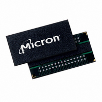
MT47H64M8CB-37E IT:B Micron Technology Inc, MT47H64M8CB-37E IT:B Datasheet - Page 96

MT47H64M8CB-37E IT:B
Manufacturer Part Number
MT47H64M8CB-37E IT:B
Description
IC DDR2 SDRAM 512MBIT 60FBGA
Manufacturer
Micron Technology Inc
Type
DDR2 SDRAMr
Datasheet
1.MT47H64M8CB-37E_ITB.pdf
(139 pages)
Specifications of MT47H64M8CB-37E IT:B
Format - Memory
RAM
Memory Type
DDR2 SDRAM
Memory Size
512M (64M x 8)
Speed
3.75ns
Interface
Parallel
Voltage - Supply
1.7 V ~ 1.9 V
Operating Temperature
-40°C ~ 85°C
Package / Case
60-FBGA
Organization
64Mx8
Density
512Mb
Address Bus
16b
Access Time (max)
500ps
Maximum Clock Rate
533MHz
Operating Supply Voltage (typ)
1.8V
Package Type
FBGA
Operating Temp Range
-40C to 85C
Operating Supply Voltage (max)
1.9V
Operating Supply Voltage (min)
1.7V
Supply Current
145mA
Pin Count
60
Mounting
Surface Mount
Operating Temperature Classification
Industrial
Lead Free Status / RoHS Status
Lead free / RoHS Compliant
ACTIVATE
Figure 46: Example: Meeting
PDF: 09005aef82f1e6e2
Rev. M 9/08 EN
Bank address
Command
Address
CK#
CK
Bank x
ACT
Row
T0
NOP
T1
Before any READ or WRITE commands can be issued to a bank within the DDR2
SDRAM, a row in that bank must be opened (activated), even when additive latency is
used. This is accomplished via the ACTIVATE command, which selects both the bank
and the row to be activated.
After a row is opened with an ACTIVATE command, a READ or WRITE command may
be issued to that row subject to the
by the clock period and rounded up to the next whole number to determine the earliest
clock edge after the ACTIVATE command on which a READ or WRITE command can be
entered. The same procedure is used to convert other specification limits from time
units to clock cycles. For example, a
clock (
(page 96), which covers any case where 5 <
also shows the case for
A subsequent ACTIVATE command to a different row in the same bank can only be is-
sued after the previous active row has been closed (precharged). The minimum time
interval between successive ACTIVATE commands to the same bank is defined by
A subsequent ACTIVATE command to another bank can be issued while the first bank is
being accessed, which results in a reduction of total row-access overhead. The mini-
mum time interval between successive ACTIVATE commands to different banks is
defined by
DDR2 devices with 8 banks (1Gb or larger) have an additional requirement:
requires no more than four ACTIVATE commands may be issued in any given
(MIN) period, as shown in Figure 47 (page 97).
t RRD
t
t
CK = 3.75ns) results in 5.3 clocks, rounded up to 6. This is shown in Figure 46
RRD (MIN) and
NOP
T2
t
RRD.
Bank y
ACT
Row
T3
t
RRD where 2 <
t
RCD (MIN)
NOP
T4
96
t RRD
t RCD
t
RCD specification.
t
RCD (MIN) specification of 20ns with a 266 MHz
NOP
T5
t
Micron Technology, Inc. reserves the right to change products or specifications without notice.
RRD (MIN)/
512Mb: x4, x8, x16 DDR2 SDRAM
t
RCD (MIN)/
Bank z
NOP
Row
T6
t
CK ≤ 3.
t
RCD (MIN) should be divided
t
CK ≤ 6. Figure 46 (page 96)
NOP
T7
© 2004 Micron Technology, Inc. All rights reserved.
NOP
T8
ACTIVATE
t
FAW. This
RD/WR
Bank y
Col
Don’t Care
T9
t
FAW
t
RC.


