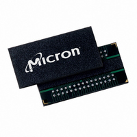
MT47H64M8CB-37E IT:B Micron Technology Inc, MT47H64M8CB-37E IT:B Datasheet - Page 110

MT47H64M8CB-37E IT:B
Manufacturer Part Number
MT47H64M8CB-37E IT:B
Description
IC DDR2 SDRAM 512MBIT 60FBGA
Manufacturer
Micron Technology Inc
Type
DDR2 SDRAMr
Datasheet
1.MT47H64M8CB-37E_ITB.pdf
(139 pages)
Specifications of MT47H64M8CB-37E IT:B
Format - Memory
RAM
Memory Type
DDR2 SDRAM
Memory Size
512M (64M x 8)
Speed
3.75ns
Interface
Parallel
Voltage - Supply
1.7 V ~ 1.9 V
Operating Temperature
-40°C ~ 85°C
Package / Case
60-FBGA
Organization
64Mx8
Density
512Mb
Address Bus
16b
Access Time (max)
500ps
Maximum Clock Rate
533MHz
Operating Supply Voltage (typ)
1.8V
Package Type
FBGA
Operating Temp Range
-40C to 85C
Operating Supply Voltage (max)
1.9V
Operating Supply Voltage (min)
1.7V
Supply Current
145mA
Pin Count
60
Mounting
Surface Mount
Operating Temperature Classification
Industrial
Lead Free Status / RoHS Status
Lead free / RoHS Compliant
Table 42: WRITE Using Concurrent Auto Precharge
PDF: 09005aef82f1e6e2
Rev. M 9/08 EN
WRITE with auto precharge
From Command
(Bank n)
cle). All of the WRITE diagrams show the nominal case, and where the two extreme
cases (
ded. Figure 60 (page 111) shows the nominal case and the extremes of
Upon completion of a burst, assuming no other commands have been initiated, the DQ
will remain High-Z and any additional input data will be ignored.
Data for any WRITE burst may be concatenated with a subsequent WRITE command to
provide continuous flow of input data. The first data element from the new burst is ap-
plied after the last element of a completed burst. The new WRITE command should be
issued x cycles after the first WRITE command, where x equals BL/2.
Figure 61 (page 112) shows concatenated bursts of BL = 4 and how full-speed random
write accesses within a page or pages can be performed. An example of nonconsecutive
WRITEs is shown in Figure 62 (page 112). DDR2 SDRAM supports concurrent auto pre-
charge options, as shown in Table 42 (page 110).
DDR2 SDRAM does not allow interrupting or truncating any WRITE burst using BL = 4
operation. Once the BL = 4 WRITE command is registered, it must be allowed to com-
plete the entire WRITE burst cycle. However, a WRITE BL = 8 operation (with auto
precharge disabled) might be interrupted and truncated only by another WRITE burst
as long as the interruption occurs on a 4-bit boundary due to the 4n-prefetch architec-
ture of DDR2 SDRAM. WRITE burst BL = 8 operations may not be interrupted or
truncated with any command except another WRITE command, as shown in Figure 63
(page 113).
Data for any WRITE burst may be followed by a subsequent READ command. To follow
a WRITE,
cycles required to meet
WRITE burst may be followed by a subsequent PRECHARGE command.
met, as shown in Figure 65 (page 115).
less of the data mask condition.
WRITE or WRITE with auto precharge
READ or READ with auto precharge
t
DQSS [MIN] and
t
PRECHARGE or ACTIVATE
WTR should be met, as shown in Figure 64 (page 114). The number of clock
To Command
(Bank m)
t
WTR is either 2 or
t
DQSS [MAX]) might not be intuitive, they have also been inclu-
110
t
Micron Technology, Inc. reserves the right to change products or specifications without notice.
WR starts at the end of the data burst, regard-
t
512Mb: x4, x8, x16 DDR2 SDRAM
WTR/
(with Concurrent Auto Precharge)
t
CK, whichever is greater. Data for any
(CL - 1) + (BL/2) +
Minimum Delay
(BL/2)
1
© 2004 Micron Technology, Inc. All rights reserved.
t
WTR
t
DQSS for BL = 4.
t
WR must be
WRITE
Units
t
t
t
CK
CK
CK


