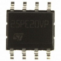
M25PE20-VMN6TP NUMONYX, M25PE20-VMN6TP Datasheet - Page 7

M25PE20-VMN6TP
Manufacturer Part Number
M25PE20-VMN6TP
Description
IC FLASH 2MBIT 75MHZ 8SOIC
Manufacturer
NUMONYX
Series
Forté™r
Datasheet
1.M25PE10-VMN6TP.pdf
(64 pages)
Specifications of M25PE20-VMN6TP
Format - Memory
FLASH
Memory Type
FLASH
Memory Size
2M (256K x 8)
Speed
75MHz
Interface
SPI, 3-Wire Serial
Voltage - Supply
2.7 V ~ 3.6 V
Operating Temperature
-40°C ~ 85°C
Package / Case
8-SOIC (3.9mm Width)
Cell Type
NOR
Density
2Mb
Access Time (max)
8ns
Interface Type
Serial (SPI)
Boot Type
Not Required
Address Bus
1b
Operating Supply Voltage (typ)
3.3V
Operating Temp Range
-40C to 85C
Package Type
SOIC N
Sync/async
Synchronous
Operating Temperature Classification
Industrial
Operating Supply Voltage (min)
2.7V
Operating Supply Voltage (max)
3.6V
Word Size
8b
Number Of Words
256K
Supply Current
8mA
Mounting
Surface Mount
Pin Count
8
Lead Free Status / RoHS Status
Lead free / RoHS Compliant
Other names
M25PE20-VMN6TPTR
Available stocks
Company
Part Number
Manufacturer
Quantity
Price
Company:
Part Number:
M25PE20-VMN6TP
Manufacturer:
MICRON
Quantity:
3 000
Company:
Part Number:
M25PE20-VMN6TP
Manufacturer:
Numonyx
Quantity:
16 500
Part Number:
M25PE20-VMN6TP
Manufacturer:
MICRON/美光
Quantity:
20 000
M25PE20, M25PE10
Table 1.
1. In the previous T7X process the pin is a Top Sector Lock input whereas in the new T9HX process, the pin
Figure 3.
1. There is an exposed central pad on the underside of the VFQFPN package. This is pulled, internally, to
2. See
C
D
Q
S
TSL or W
Reset
V
V
Figure 1.
CC
SS
is a Write Protect input (see
V
SS
Reset
, and must not be allowed to be connected to any other voltage or signal line on the PCB.
TSL
Signal name
Package mechanical
D
C
S
(1)
Signal names
VFQFPN and SO connections
Logic diagram - previous T7X
process
V CC
V SS
M25PE20
M25PE10
section for package dimensions, and how to identify pin-1.
Serial Clock
Serial Data input
Serial Data output
Chip Select
Top Sector Lock or Write Protect
Reset
Supply voltage
Ground
Figure 1
TSL or W
and
AI09713
V SS
Figure
Q
Q
S
M25PE20
M25PE10
1
2
3
4
2).
Function
Figure 2.
8
7
6
5
Reset
V CC
Reset
C
D
W
D
C
S
Logic diagram - new T9HX
process
AI09715b
V CC
V SS
M25PE10
M25PE20
Input
Input
Output
Input
Input
Input
–
–
Direction
Description
AI13808
Q
7/64


